Very small image sensor

Active Publication Date: 2009-10-29
STMICROELECTRONICS SRL
View PDF0 Cites 59 Cited by
  • Summary
  • Abstract
  • Description
  • Claims
  • Application Information

AI Technical Summary

Benefits of technology

[0015]Another object of an embodiment of the present invention is to provide a photodiode

Problems solved by technology

First, the size decrease of collection areas increases the risk of interferences, also called crosstalk, between the different photodiodes. Indeed, if the photodiodes are very close to one another, electrons intended to reach a given photodiode can be more easily attracted by a neighboring photodiode.
F

Method used


Image

  • Very small image sensor
  • Very small image sensor
  • Very small image sensor

Examples


Embodiment Construction

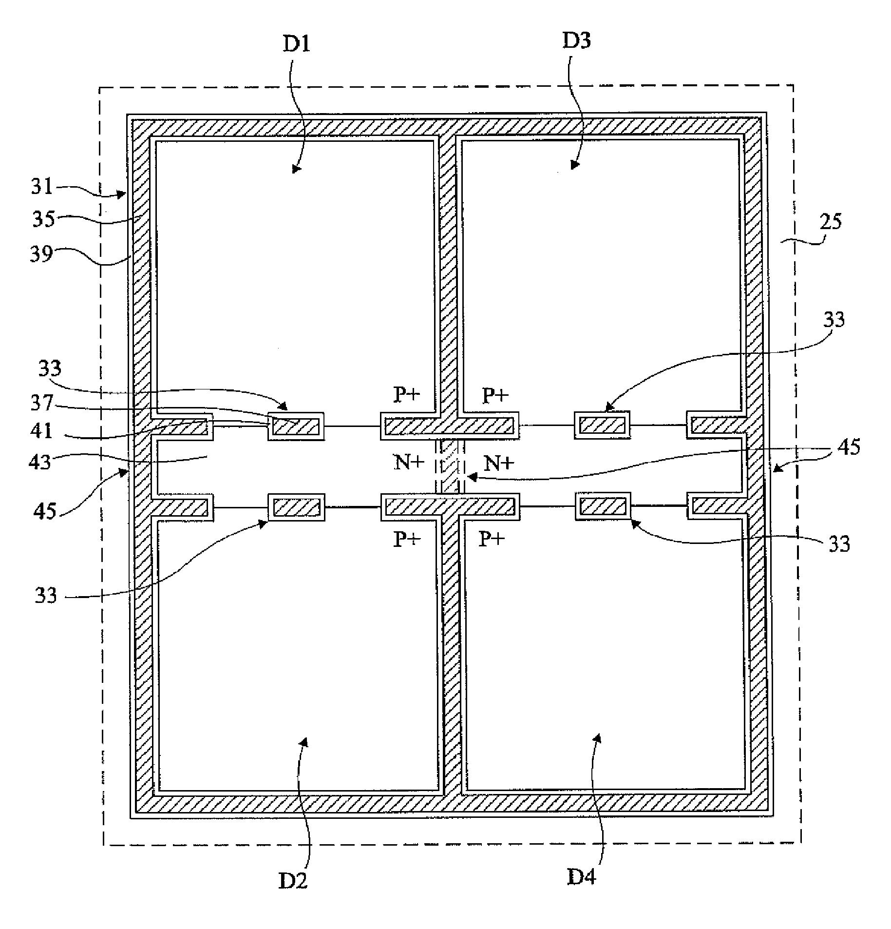
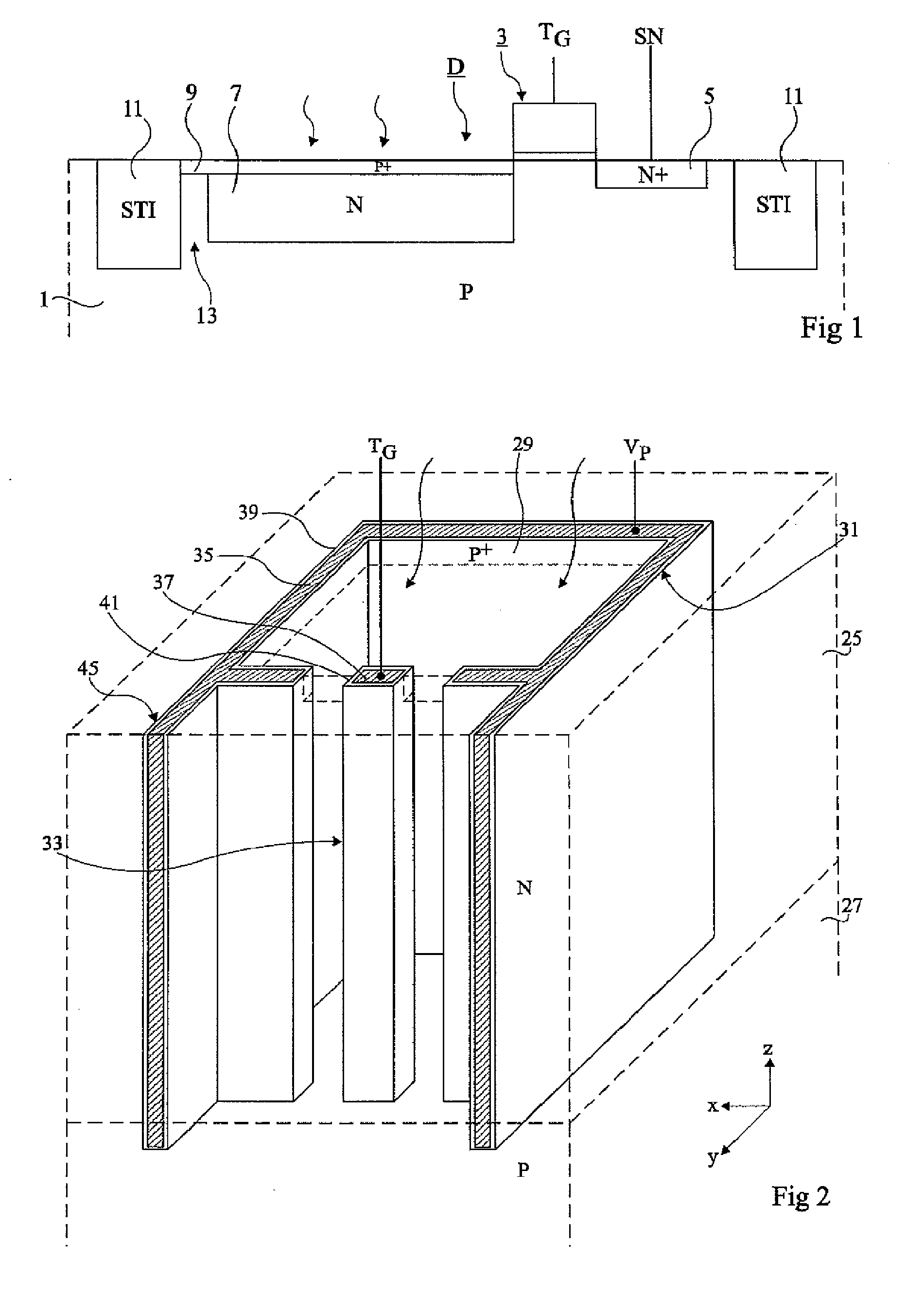
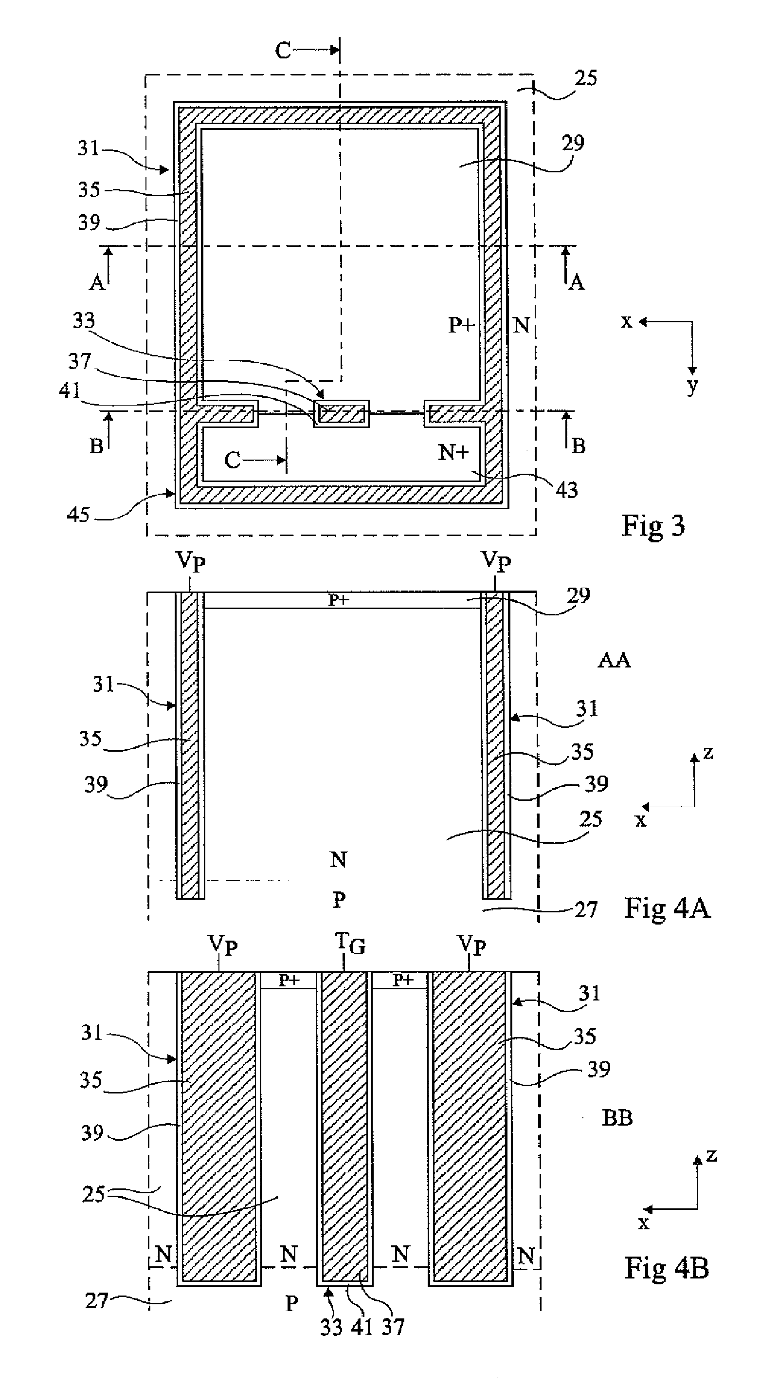
[0036]For clarity, the same elements have been designated with the same reference numerals in the different drawings. Further, as usual in the representation of integrated circuits, the various drawings are not to scale.

[0037]FIG. 1 is a simplified cross-section view of a photodiode associated with a charge transfer system of a conventional image sensor.

[0038]An insulated gate structure 3 is formed on a lightly-doped P-type semiconductor substrate 1. N-type drain and source regions 5 and 7 are located on either side of gate 3, at the surface of substrate 1. Drain region 5, to the right of gate 3, is heavily N-type doped (N+). Source region 7 is formed on a larger surface area than drain region 5. Source region 7 forms, with substrate 1, the junction of a photodiode D. Gate 3 and drain 5 are linked to metallizations (not shown) which enable putting these regions respectively in contact with a transfer control signal (TG) and with a read and processing circuit (read node SN). Photodio...


PUM


Abstract

An image sensor formed in a semiconductor stack of a lower region of a first conductivity type and of an upper region of a second conductivity type, including: a photodiode formed of a first portion of the stack; a read area formed of a second portion of the stack; a trench with insulated walls filled with a conductive material, the trench surrounding the photodiode and the read area and being interrupted, all along its height, on a portion facing the photodiode and the read area; and first connection mechanism associated with the conductive material of the trench and capable of being connected to a reference bias voltage.

Description

CROSS REFERENCE TO RELATED APPLICATIONS[0001]This application claims the priority benefit of French patent application Ser. No. 08 / 52759, filed on Apr. 24, 2008, entitled “VERY SMALL IMAGE SENSOR,” which is hereby incorporated by reference to the maximum extent allowable by law.BACKGROUND OF THE INVENTION[0002]1. Field of the Invention[0003]The present invention relates to an image sensor made in monolithic form for use in image shooting devices.[0004]More specifically, the present invention relates to an image sensor formed of small elements.[0005]2. Discussion of the Related Art[0006]Conventionally, a monolithic image sensor comprises photodiodes and transistors formed in a silicon substrate. More specifically, each pixel of an image sensor comprises a photodiode associated with a transfer transistor having its drain region associated with a read and processing circuit comprising one or several transistors. An insulation trench extending from the substrate surface enables insulati...

Claims


Application Information

Patent Timeline
IPC IPC(8): G01J1/44H01L31/101
CPCH01L27/1463H01L27/14641H01L27/14687H01L27/14643
Inventor ROY, FRANCOISRAMADOUT, BENOIT
Owner STMICROELECTRONICS SRL
Why Eureka
Try Eureka