
Integrated device

a technology of integrated devices and batteries, applied in the direction of semiconductor devices, basic electric elements, electrical equipment, etc., can solve the problems of high cost, relative thick and expensive packaging, etc., and achieve the effect of improving the sealing property of the battery and laminate better

Inactive Publication Date: 2009-10-29
KONINKLIJKE PHILIPS ELECTRONICS NV
View PDF5 Cites 31 Cited by
  • Summary
  • Abstract
  • Description
  • Claims
  • Application Information

AI Technical Summary

Benefits of technology

[0005]It is an object of the present invention to overcome this problem, and to provide an improved, integrated device with reduced thickness.
[0008]Thus, the prefabricated battery gets the function also to act as top encapsulation of the device or act as a supporting and / or protective substrate of the device. This yields a thinner and more robust device compared to prior art structures since a separate encapsulation / substrate can be omitted. Due to the battery, the device may operate autonomously.
[0010]In one embodiment, the substrate is a transparent substrate, the at least one active organic element is processed on the transparent substrate, and the prefabricated thin battery is arranged on top of the at least one active organic element. Thus, here the prefabricated battery acts as the encapsulation of the integrated device. Further, the transparent substrate can be made of a flexible material, allowing the complete device to be flexible.
[0014]In another embodiment, the at least one active organic element is an organic photovoltaic cell, and the photovoltaic cell is adapted to charge the battery. In another embodiment, the at least one active organic element comprises an OLED and an organic photovoltaic cell arranged adjacent to each other, the organic photovoltaic cell is adapted to charge the battery, and the battery is adapted to power the OLED. The adjacent OLED and organic photovoltaic cell can advantageously be processed on the same substrate at the same time, which is very cost efficient.
[0016]In one embodiment, a fixing agent is applied around the at least one active organic element and between the at least one active organic element and the prefabricated thin battery, which fixing agent comprises a getter material. The getter material is a water absorbing material, such as calcium oxide. Thus, the fixing agent serves to join the at least one active organic element and the prefabricated thin battery, as well as to protect the at least one active organic element from moisture from the sides of the device.
[0019]In one embodiment, the method further comprises filling the battery with electrolyte after the battery is laminated on top of the at least one active organic element. Before the battery is filled with the electrolyte, it is much flatter and will therefore laminate better, which in turn improves the sealing property of the battery.

Problems solved by technology

However, the structure disclosed in WO03019658 yields a relatively thick and expensive package since the energy carrier and the OLED are encapsulated and sealed separately.
Also, the energy carrier is fabricated with a thin film technology, which results in high cost.

Method used


Image

  • Integrated device
  • Integrated device

Examples


Embodiment Construction

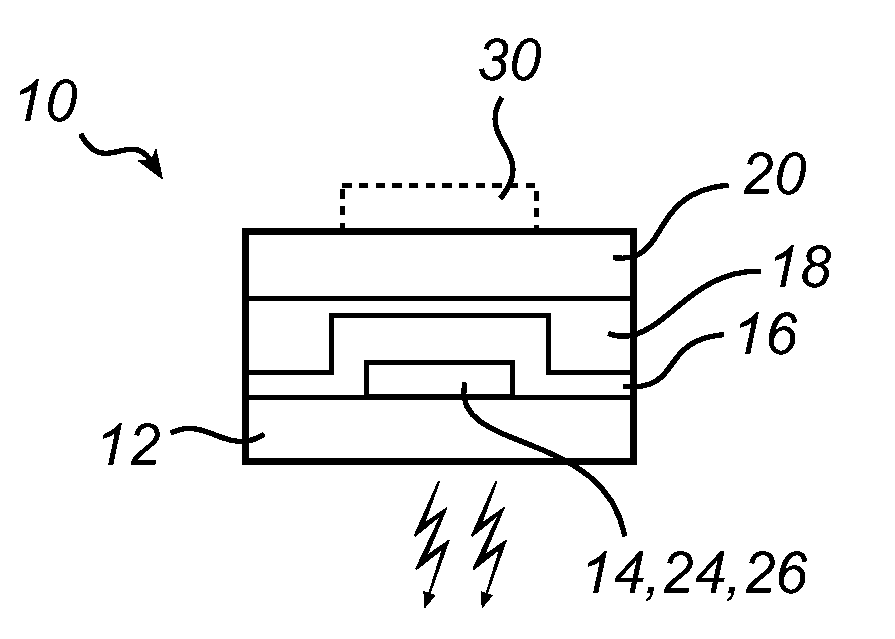
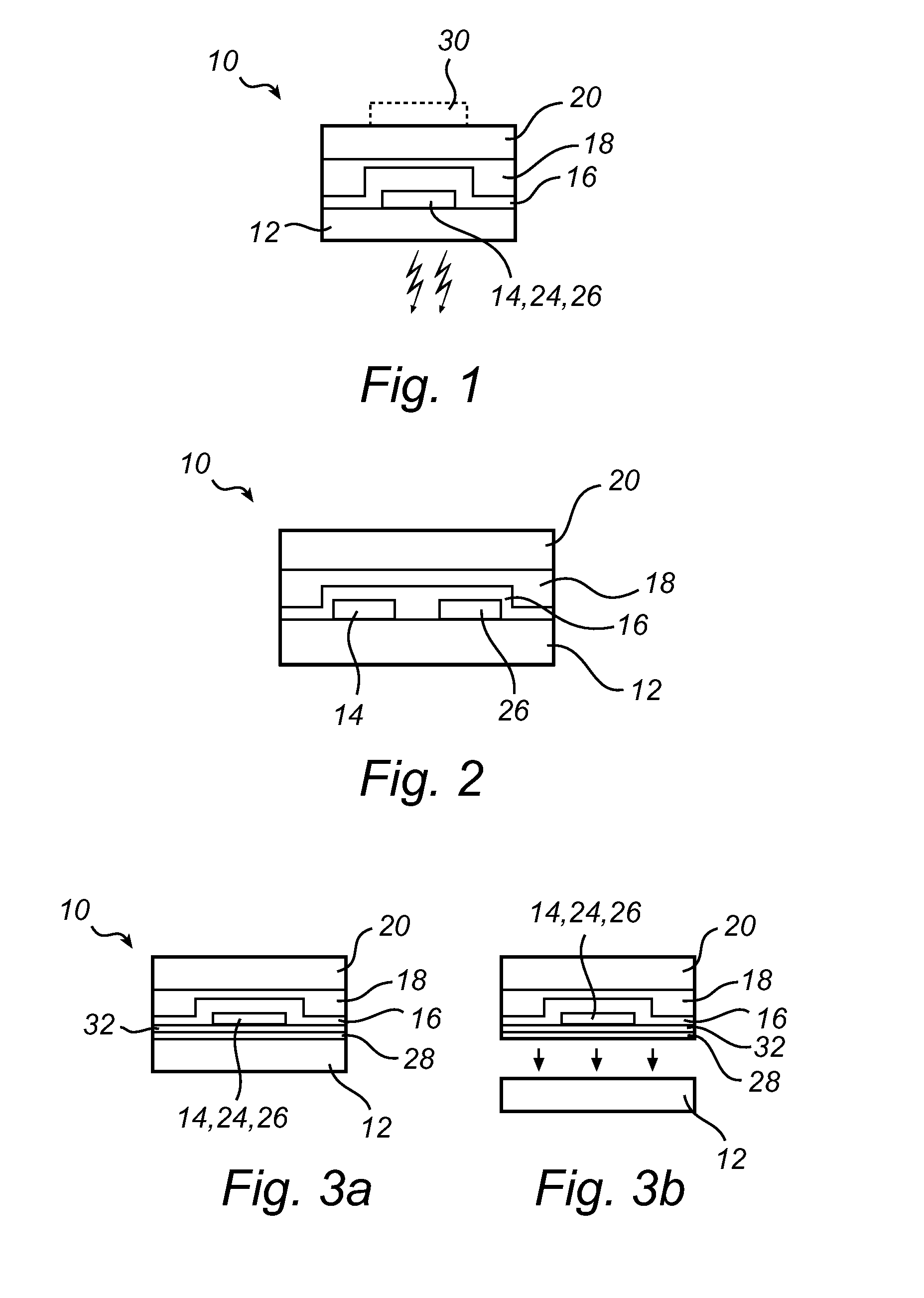
[0024]FIG. 1 is a cross-sectional side view of an integrated device 10 according to an embodiment of the invention. From bottom to top in FIG. 1, the integrated device 10 comprises a transparent substrate 12 onto which an organic light emitting diode (OLED) 14 is processed. The OLED 14 may be processed by means of printing or deposition or evaporation through a shadow mask, for example. The transparent substrate 12 may be made glass or plastics, for example. Also, it can be made of a flexible material, allowing the complete device 10 to be flexible, and the OLED 14 may function as a display or as a light source.

[0025]The substrate 12 and the OLED 14 are coated with a thin-film packaging layer 16, for example a NONON-stack (silicon nitride-silicon oxide-silicon nitride-silicon oxide-silicon nitride). On the layer 16, a topcoat 18 is applied, and on top of the topcoat 18, a prefabricated thin battery 20 is attached. The prefabricated thin battery 20 covers the complete OLED area. The ...


PUM

PropertyMeasurementUnit
thicknessaaaaaaaaaa
thicknessaaaaaaaaaa
thicknessaaaaaaaaaa

Abstract

The present invention relates to an integrated device (10) comprising at least one active organic element (14, 24, 26), a substrate supporting the at least one active organic element, a prefabricated thin battery (20) coupled to the at least one active organic element, and an encapsulation for sealing the integrated device, wherein one of the substrate and the encapsulation is formed by the prefabricated thin battery. This structure allows for a thin integrated device. The present invention also relates to a method for the manufacturing of such an integrated device.

Description

TECHNICAL FIELD OF THE INVENTION[0001]The present invention relates to an integrated device comprising at least one active organic element and a thin battery coupled to the at least one active organic element. The present invention also relates to a method for the manufacturing of such an integrated device.BACKGROUND OF THE INVENTION[0002]An example of a device comprising an active organic element and a battery is disclosed in the document WO03019658. More precisely, the device in WO03019658 comprises, from bottom to top, a substrate (such as glass or a flexible film), an energy carrier (battery or photovoltaic cell), a semitransparent insulation layer serving as a substrate for an organic light emitting diode (OLED), and finally an encapsulation or seal, which is comprised of glass. Upon operation, the energy carrier supplies a voltage that causes the OLED to emit light.[0003]In one particular embodiment, the energy carrier and the OLED are produced on opposite sides of the semitra...

Claims


Application Information

Patent Timeline
Patent Type & Authority Applications(United States)
IPC IPC(8): H01M14/00
CPCH01L27/288H01L51/524H01L27/3225H01L27/305H10K65/00H10K39/30H10K59/871H10K59/874H10K50/841H10K59/00
Inventor LIFKA, HERBERTDORTMANS, ALBERTUS ADRIANUS MARIAMEULENKAMP, ERIC ALEXANDERTANASE, CRISTINA
Owner KONINKLIJKE PHILIPS ELECTRONICS NV
Learn More