

Solar Cell Design and Methods of Manufacture
a solar cell and design technology, applied in the field of solar cell design and manufacture, can solve the problems of small sun energy receipt, high cost of solar cell silicon, and difficult manufacturing of tubular solar cells, and achieve the effect of improving efficiency
- Summary
- Abstract
- Description
- Claims
- Application Information
AI Technical Summary
Benefits of technology
Problems solved by technology
Method used
Image

Examples
example 1
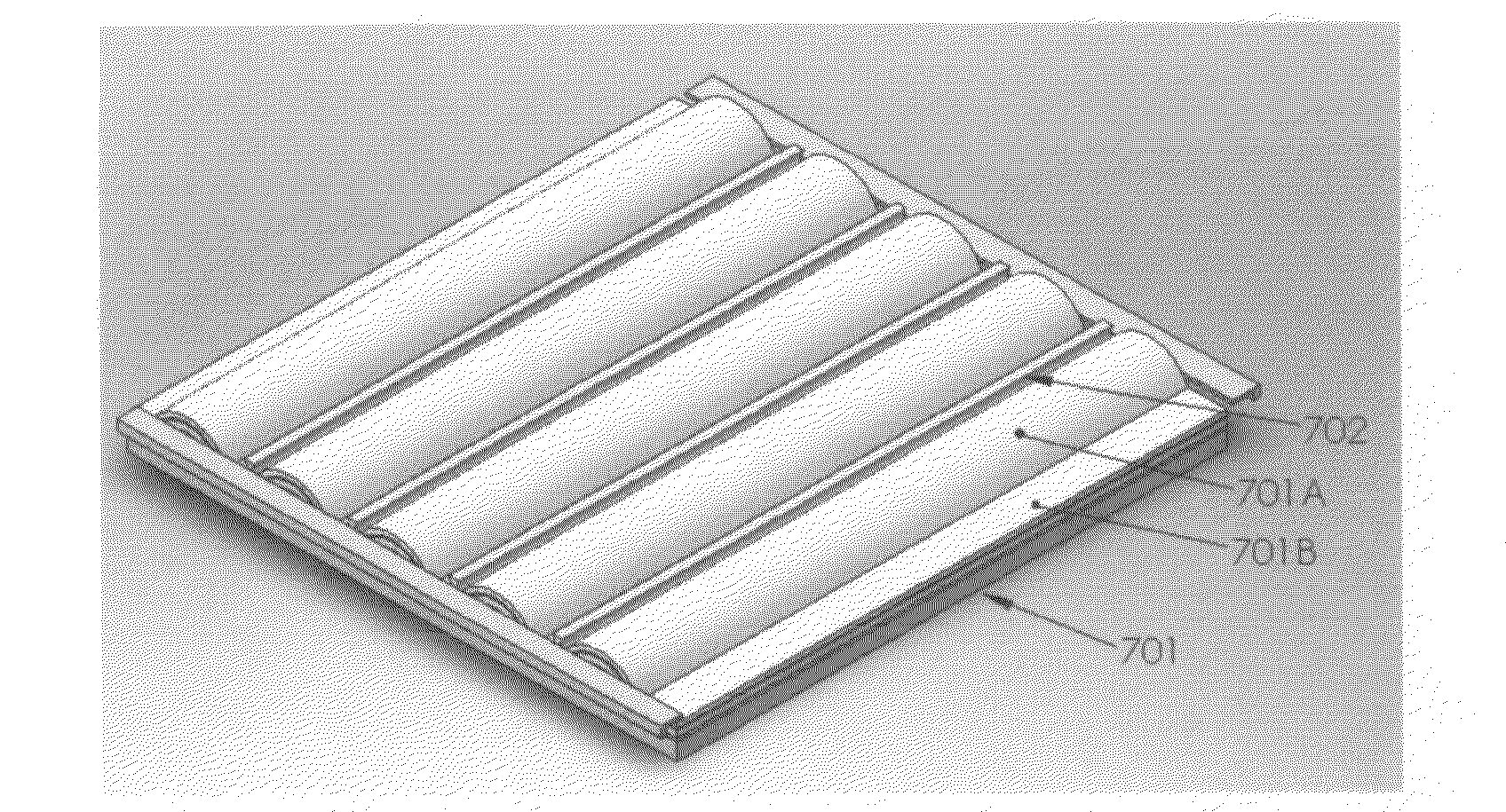
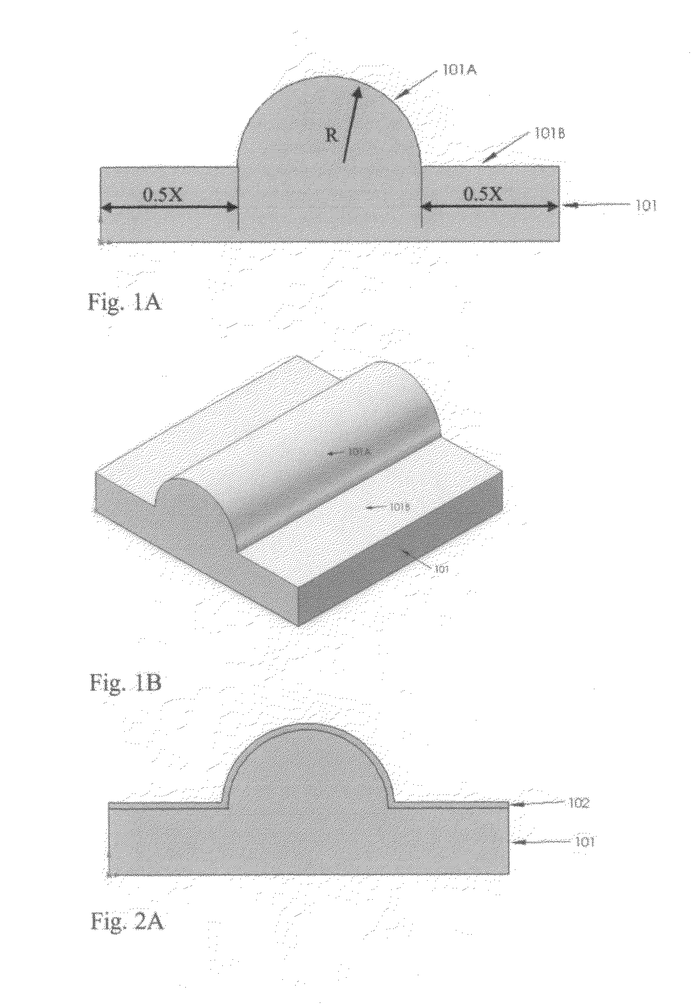
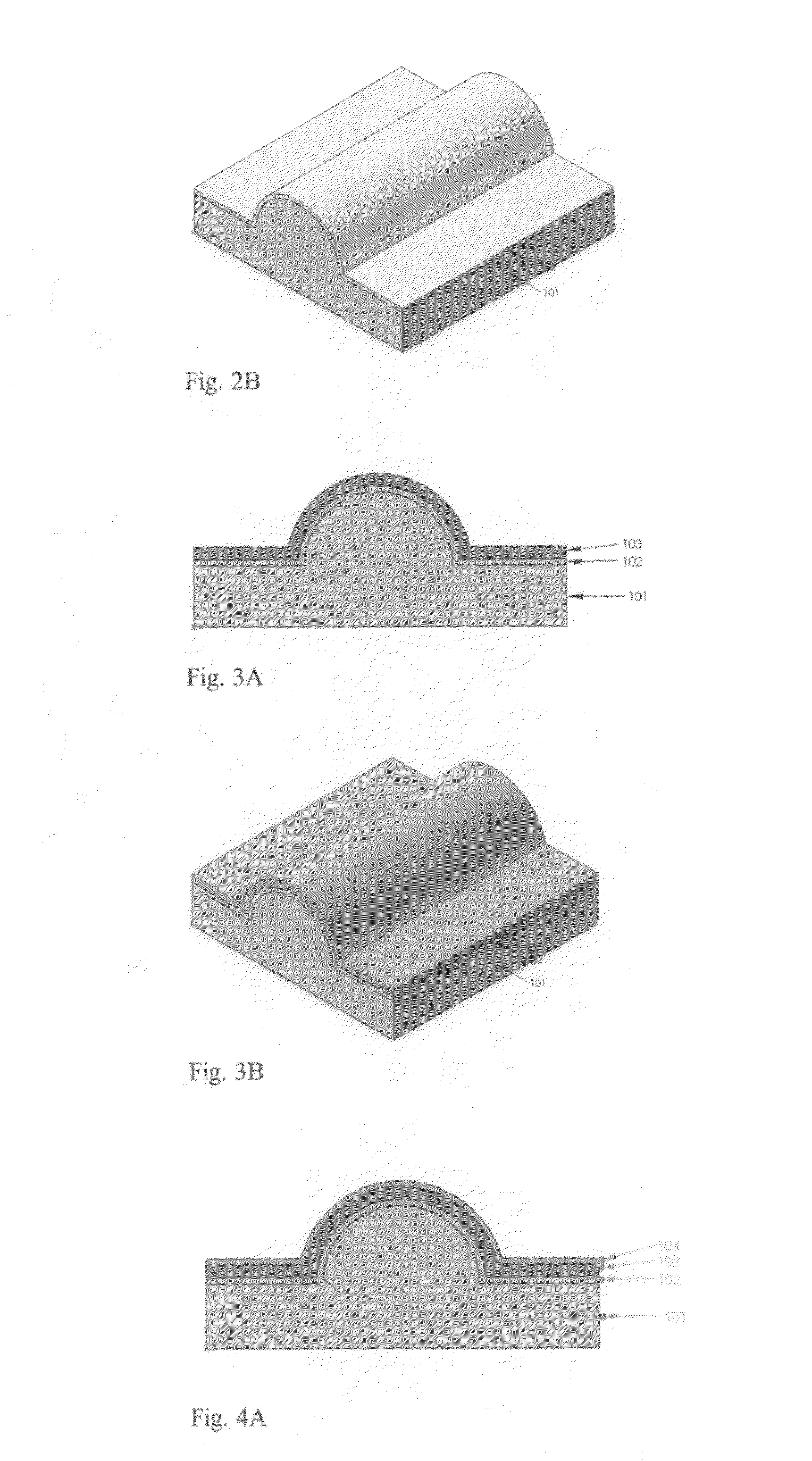
[0072]A stainless steel sheet was formed to have 5 semi-cylindrical arrays with flattened areas between them. The radius of the semi-cylindrical area was 5 mm. The flattened area between the two semi-cylindrical areas was 6 mm width. The substrate dimension was 100 mm length and 100 mm width Grid array CIGS solar cells were formed on the substrate. The first step was to vacuum deposit a MoCu alloy back contact electrode followed by mechanical cutting to form patterns. Then, Cu(InGa)Se2 semiconductor layer was formed by co-evaporating process under vacuum condition. CdS thin film was then deposited on the Cu(InGa)Se2 surface by chemical deposition method. ZnO thin film was then vacuum deposited on the CdS surface followed by second mechanical cutting to form patterns. ZnO:Al thin film was then deposited on the ZnO surface and finally ZnO:Al was partially removed by mechanical cutting. Total 25 solar cells were formed on the substrate with 5×5 grid array format.
example 2
[0073]A soda lime glass substrate was formed to have 5 semi-cylindrical arrays with flattened areas between them. The radius of the semi-cylindrical area was 5 mm. The flattened area width between the two semi-cylindrical areas was 6 mm. The substrate dimension was 100 mm length and 100 mm width. Grid array CIGS solar cells were formed on the substrate. The first step was to vacuum deposit a MoCu alloy back contact electrode followed by mechanical cutting to form patterns. Then, a thin copper layer is deposited on MoCu surface. Cu(InGa)Se2 semiconductor layer was then formed by sequentially electroplating a stack of Cu / In / Ga / Se followed by annealing it at 550 C for 35 minutes under N2 environment. CdS thin film was then deposited on the Cu(InGa)Se2 surface by chemical deposition method. ZnO thin film was then deposited on the CdS surface followed by second mechanical cutting to form patterns. ZnO:Al thin film was then deposited on the ZnO surface and finally ZnO:Al thin film layer w...
example 3
[0074]A stainless steel sheet was formed to have 5 semi-cylindrical arrays with flattened areas between the semi-cylindrical areas. The radius of the semi-cylindrical area was 5 mm. The flattened area between the two semi-cylindrical areas was 6 mm. The substrate dimension is 100 mm length and 100 mm width. Grid array CIGS solar cells were formed on the substrate. The first step was to vacuum deposit a MoCu alloy back contact electrode followed by mechanical cutting to form patterns. A thin Cu layer was then deposited on the CuMo surface. Cu(InGa)Se2 semiconductor layer was then formed by sequentially electroplating a stack of Cu / In / Ga / Se followed by annealing it at 550 C for 35 minutes under N2 environment. CdS thin film was then deposited on the Cu(InGa)Se2 surface by chemical deposition bath method. ZnO thin film was then vacuum deposited on the CdS surface followed by second mechanical cutting to form patterns. ZnO:Al thin film was then deposited on the ZnO surface and finally Z...
PUM
 Abstract
Description
Claims
Application Information