Chip package structure and method of making the same
Inactive Publication Date: 2009-11-05
WALSIN LIHWA
View PDF33 Cites 24 Cited by
Summary
Abstract
Description
Claims
Application Information
AI Technical Summary
This helps you quickly interpret patents by identifying the three key elements:
Problems solved by technology
Method used
Benefits of technology
[0009]It is therefore one of the objectives of the present invention to provide a chip package and a fabrication method thereof to
Problems solved by technology
First, the heat dissipation efficiency of conventional LED chip package is low.
Whether the LED chip package is a leadframe type or a PCB type, the package substrate and the package resin are poor heat dissipation materials such as plastic or resin, and heat produced while light is emitted by the LED chips may not be quickly and efficiently dissipated.
However, the bonding wire i
Method used
Image
Click on the blue label to locate the original text in one second.
Reading with bidirectional positioning of images and text.
Examples
Example
[0056]To provide a better understanding of the presented invention, preferred embodiments will be made in details. The preferred embodiments of the present invention are illustrated in the accompanying drawings with numbered elements.
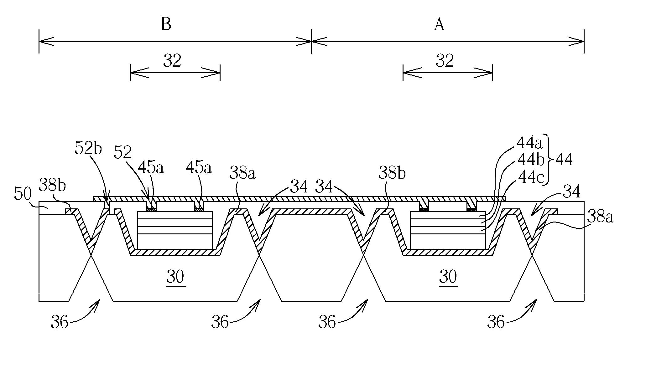
[0057]Please refer to FIG. 3 to FIG. 10. FIG. 3 to FIG. 10 are schematic views of a method of making a chip package according to a preferred embodiment of the present invention. FIG. 3a to FIG. 10a are either top views or bottom views, while FIG. 3b to FIG. 10b and FIG. 4c are cross-sectional views. As shown in FIG. 3a and FIG. 3b, a package substrate 30 having a plurality of units U defined thereon is provided at first. In the present embodiment, the thickness of the package substrate 30 is about 1000 micrometers (μm), but is not limited. The package substrate 30 may be a semiconductor substrate, for instance a silicon substrate, gallium arsenide (GaAs) substrate, or other substrates with good heat conductivity, suitable for batch production (large sca...
PUM
Abstract
A chip package structure and method thereof uses a semiconductor substrate as a package substrate, which improve heat dissipation. Also, the chip package structure is incorporated with a planarization structure, which renders the chip and the package substrate a substantially planar surface, thereby making formation of a planar patterned conductive layer possible. Accordingly, electrical connections in series or in parallel between chips can be easily implemented by virtue of the planar patterned conductive layer.
Description
CROSS REFERENCE TO RELATED APPLICATIONS[0001]This application is a continuation-in-part of applicant's earlier applications, Ser. No. 11 / 611,892, filed Dec. 18, 2006, Ser. No. 11 / 612,486, filed Dec. 19, 2006, Ser. No. 11 / 612,490, filed Dec. 19, 2006, Ser. No. 11 / 612,491, filed Dec. 19, 2006, and Ser. No. 12 / 481,578, filed Jun. 10, 2009, which is a continuation-in-part of application Ser. No. 11 / 611,892, filed Dec. 18, 2006, Ser. No. 11 / 612,486, filed Dec. 19, 2006, Ser. No. 11 / 612,490, filed Dec. 19, 2006, and Ser. No. 11 / 612,491, filed Dec. 19, 2006, the entireties of which are incorporated by reference.BACKGROUND OF THE INVENTION[0002]1. Field of the Invention[0003]The present invention is related to a chip package and the method of making the same, and more particularly, to a chip package utilizing a semiconductor substrate as a package substrate and having good heat conductivity while able to fulfill electrical connection of a plurality of chips in series or in parallel easily a...
Claims
Application Information
Patent Timeline
Application Date:The date an application was filed.
Publication Date:The date a patent or application was officially published.
First Publication Date:The earliest publication date of a patent with the same application number.
Issue Date:Publication date of the patent grant document.
PCT Entry Date:The Entry date of PCT National Phase.
Estimated Expiry Date:The statutory expiry date of a patent right according to the Patent Law, and it is the longest term of protection that the patent right can achieve without the termination of the patent right due to other reasons(Term extension factor has been taken into account ).
Invalid Date:Actual expiry date is based on effective date or publication date of legal transaction data of invalid patent.