Optimum structure for charge pump circuit with bipolar output

a charge pump and bipolar output technology, applied in the field of charge pumps, can solve the problems of reducing the design area, wasting precious design area, and reducing the charge conversion efficiency, so as to reduce the total cost, and save the design area. effect of huge area

Inactive Publication Date: 2009-11-05
AMAZING MICROELECTRONICS
View PDF9 Cites 32 Cited by
  • Summary
  • Abstract
  • Description
  • Claims
  • Application Information

AI Technical Summary

Benefits of technology

[0008]An object of the present invention is to provide a charge pump circuit with bipolar output, which comprises minimum number switches and capacitors, and driven with four-phase clock. The proposed new charge pump circuit provides higher bipolar voltage than single power source input diminish the total cost and save huge design area in an IC, which meets the requirement for several high voltages application in an IC or I / O interface.
[0009]Another object of the present invention is to provide a charge pump circuit with bipolar output, which has the advantages of both high conversion efficiency and smaller ripple of output voltage.

Problems solved by technology

Regardless of what type of charge pump circuits mentioned above, they have the drawbacks of both limited charge conversion efficiency and large ripple of output voltage.
Moreover, the above-mentioned charge pump circuits include too many capacitors and switches, which increase the total cost and waste the precious design area.

Method used


Image

  • Optimum structure for charge pump circuit with bipolar output
  • Optimum structure for charge pump circuit with bipolar output
  • Optimum structure for charge pump circuit with bipolar output

Examples


Embodiment Construction

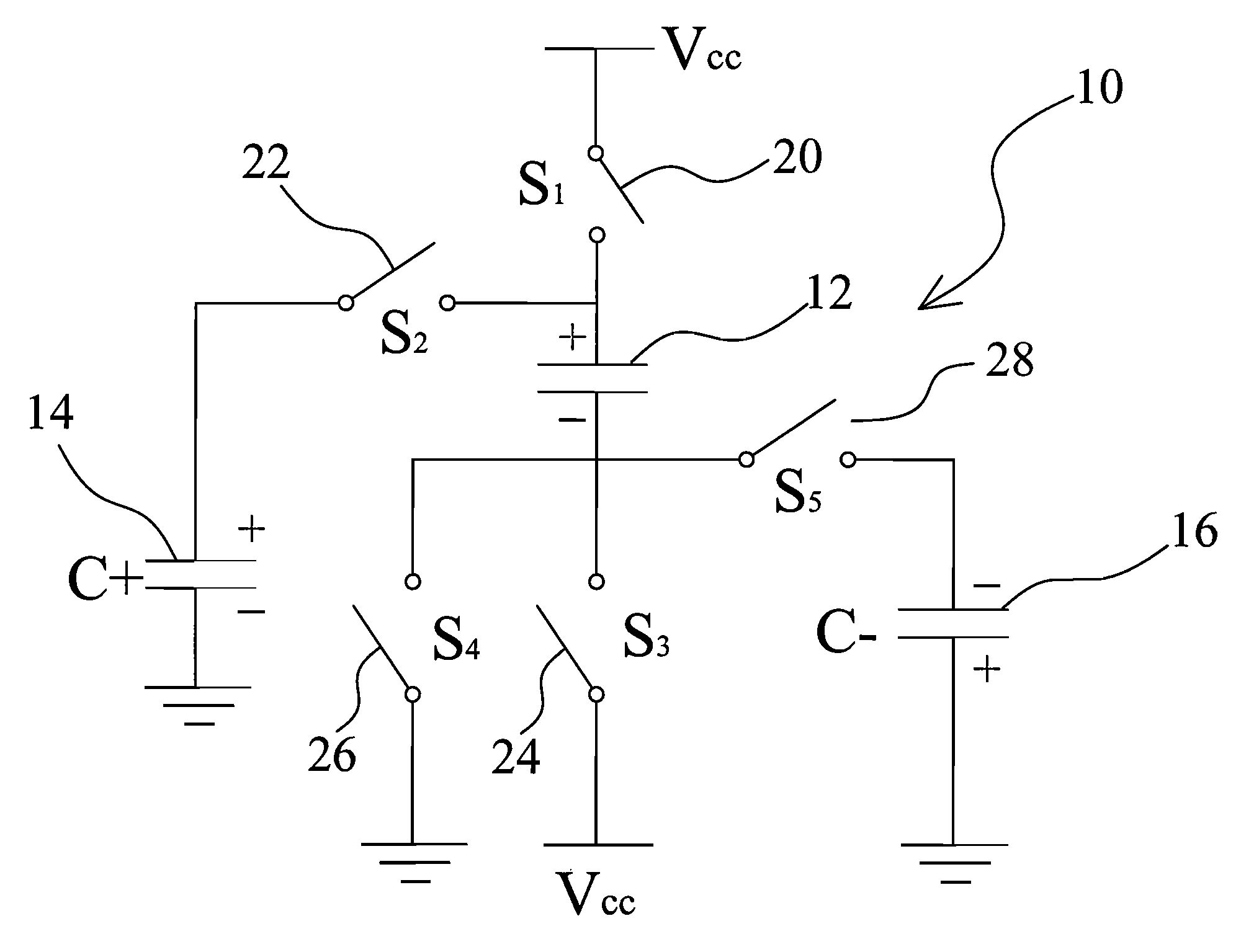
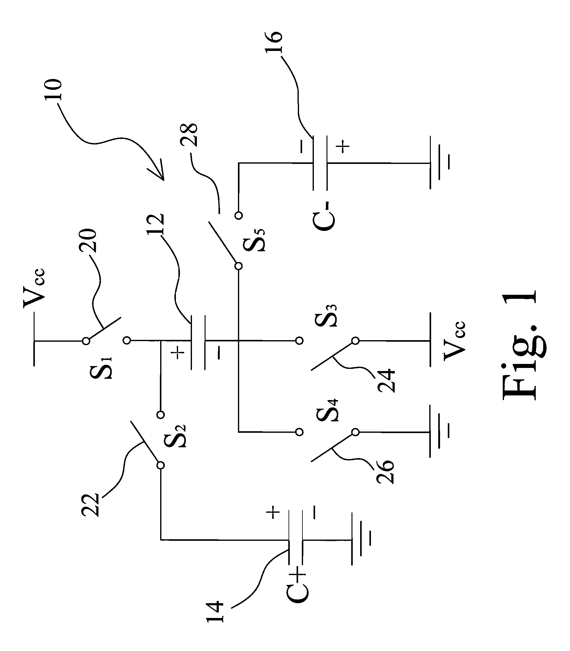
[0015]The present invention discloses a charge pump circuit with bipolar output, which includes minimum capacitors and switches and can apply to the present CMOS IC process. This charge pump circuit is composed of five switches, three capacitors and a power source, and makes use of four-phase clock signals to produce bipolar voltage higher than the input voltage. The proposed charge pump circuit meets the requirement that several high voltages for circuits in an IC or I / O circuits of an IC needed under the condition of a single power source.

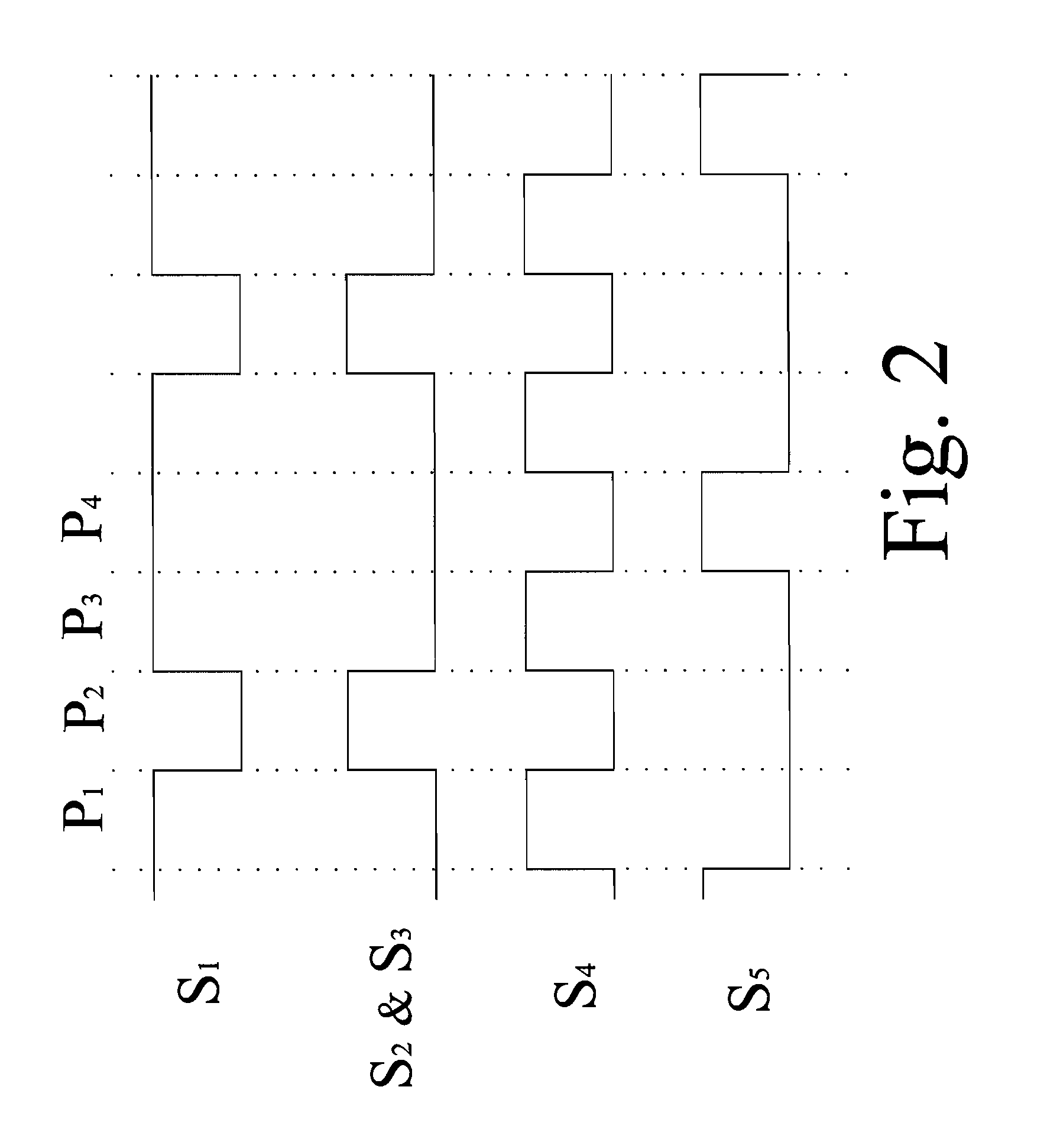
[0016]Please refer to FIG. 1. FIG. 1 is a diagram of a charge pump circuit of the present invention. As shown in FIG. 1, a charge pump circuit 10 comprises one transfer capacitor 12(C1), two storage capacitors 14 (C+) and 16 (C−), and five switches 20, 22, 24, 26, 28 (S1˜S5), and provides an input voltage collocated with clock signals to control the turn-on time of the switches in order to adjust the level of the output voltage and thus produce b...


PUM


Abstract

A charge pump circuit with bipolar output comprises a first switch capable of selectively connecting a first input terminal of a transfer capacitor to a voltage source, a second switch capable of selectively connecting a first input terminal of a first storage capacitor to said first input terminal of said transfer capacitor; a third switch capable of selectively connecting a second input terminal of said transfer capacitor to said voltage source; a fourth switch selectively connecting said second input terminal of said transfer capacitor to a ground terminal; and a fifth switch selectively connecting said second input terminal of said transfer capacitor to a second input terminal of a second storage capacitor. The charge pump circuit is collocated with clock signals to be selectively driven by a four-phase signal so as to produce bipolar voltages with magnitudes higher than the input voltage with minimum number of switches and capacitors and also accomplish the highest efficiency.

Description

BACKGROUND OF THE INVENTION[0001]1. Field of the Invention[0002]The present invention relates to a charge pump and, more particularly, to a charge pump circuit with bipolar output that includes minimum number of capacitors and switches and can be applied to existent CMOS IC fabrication processes.[0003]2. Description of Related Art[0004]With the development of the manufacturing process, the size and operating voltage of components become smaller. However, the transmission voltages of I / O signals usually are higher than those of internal circuits or applied voltages. Therefore, it is necessary to design a DC voltage conversion circuit in an IC to provide a voltage source with a voltage higher than the applied voltage. Charge pump circuit is one of the DC voltage conversion circuit.[0005]Because the charge pump circuits proposed here have the function of converting a unipolar voltage (+V) to a bipolar voltage output (+ / −V) or a bipolar double voltage output (+ / −2V), they can be widely ...

Claims


Application Information

Patent Timeline
Patent Type & Authority Applications(United States)
IPC IPC(8): H02M3/07
CPCH02M2003/075H02M3/073H02M3/075
Inventor TSENG, TANG-KUEIJIANG, RYAN HSIN-CHIN
Owner AMAZING MICROELECTRONICS
Why Eureka
Try Eureka