Semiconductor device and method for manufacturing semiconductor device

a semiconductor and semiconductor technology, applied in the direction of solid-state devices, basic electric elements, thermoelectric devices, etc., can solve the problems of increasing thickness and size of semiconductor devices, and achieve the effects of high reliability, reduced thickness and size, and toleran

Inactive Publication Date: 2009-11-12
SEMICON ENERGY LAB CO LTD
View PDF45 Cites 31 Cited by
  • Summary
  • Abstract
  • Description
  • Claims
  • Application Information

AI Technical Summary

Benefits of technology

[0007]Therefore, an object is to provide a highly reliable semiconductor device that is reduced in thickness and size and has tolerance for external stress and electrostatic discharge. Further, another object is to manufacture a semiconductor device with high yield by preventing a defect in shape and characteristic in a manufacturing process.
[0042]With the use of a conductive layer covering (overlapping) a semiconductor integrated circuit, electrostatic breakdown (malfunctions of the circuit or damages of a semiconductor element) due to electrostatic discharge of the semiconductor integrated circuit is prevented. Further, with the use of a pair of impact diffusion layers and impact resistance layers which sandwich the semiconductor integrated circuit, a highly reliable semiconductor device that is reduced in thickness and size and has tolerance can be provided. Further, shape defects and defective characteristics are prevented in the manufacturing process, so that a semiconductor device can be manufactured with high yield.

Problems solved by technology

However, there occurs a problem that by providing reinforcing metal plates as in Patent Document 1, a semiconductor device is increased in thickness and size.

Method used


Image

  • Semiconductor device and method for manufacturing semiconductor device
  • Semiconductor device and method for manufacturing semiconductor device
  • Semiconductor device and method for manufacturing semiconductor device

Examples


embodiment 1

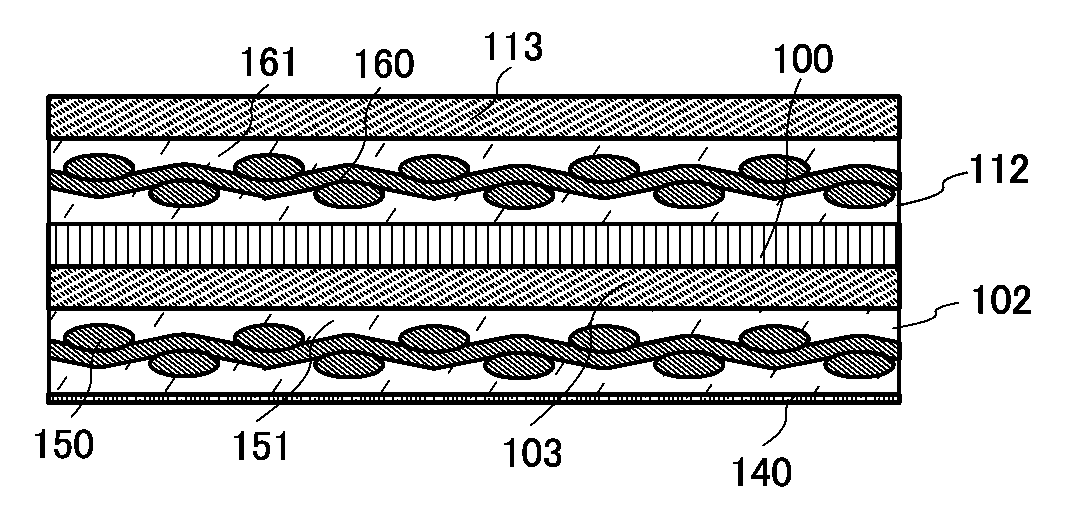
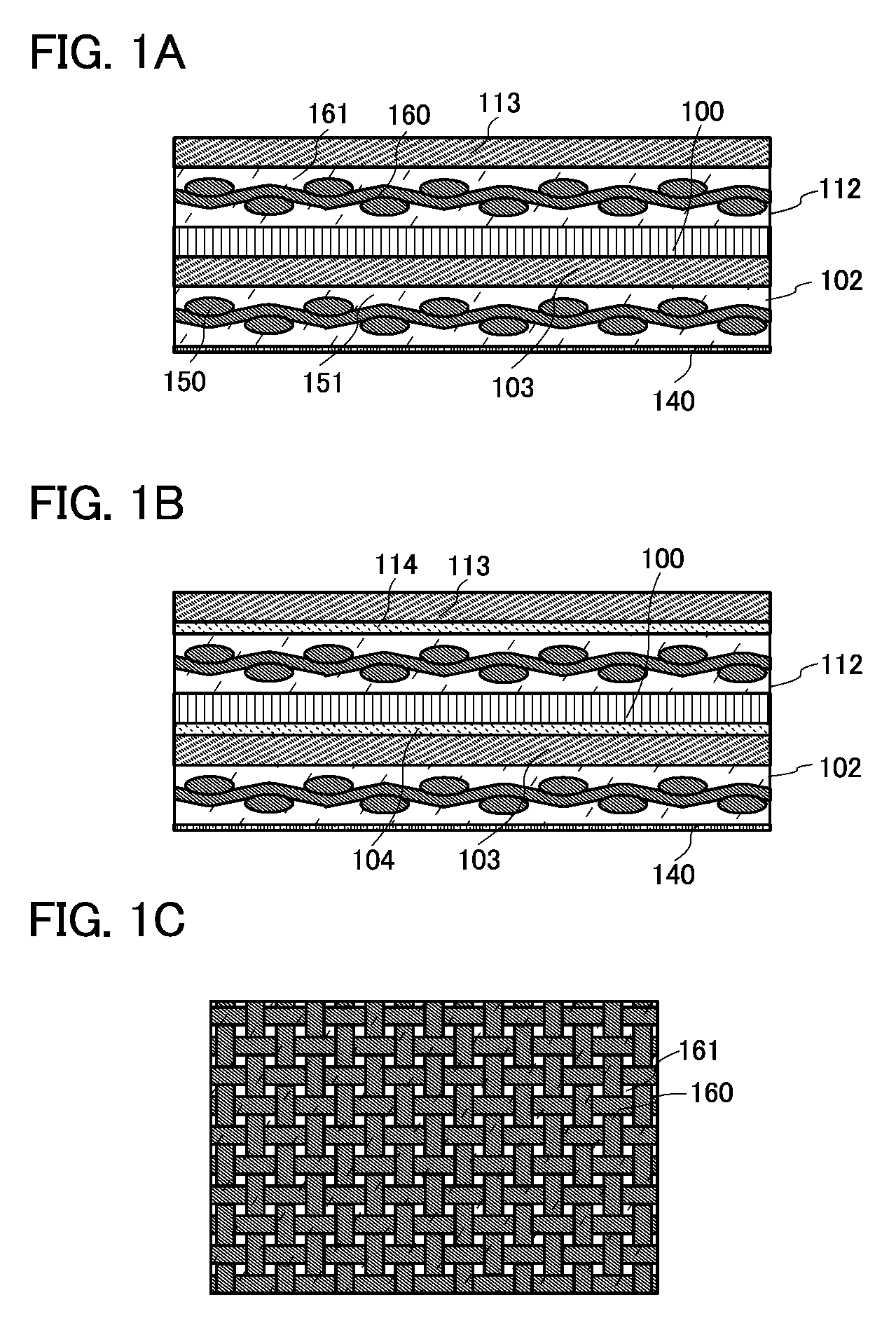
[0082]In this embodiment, a highly reliable semiconductor device and a high-yield method for manufacturing a semiconductor device are described in detail with reference to FIGS. 1A to 1C, FIGS. 2A and 2B, and FIGS. 3A to 3D.

[0083]In a semiconductor device according to this embodiment, a semiconductor integrated circuit is separated from a substrate over which the semiconductor integrated circuit has been formed and is sandwiched between flexible impact resistance layers. Note that in this specification, the substrate over which the semiconductor integrated circuit has been formed is also referred to as a formation substrate. Thus, the semiconductor integrated circuit is formed over the formation substrate with a separation layer interposed therebetween.

[0084]FIGS. 1A and 1B each illustrate a semiconductor device according to this embodiment. In FIG. 1A, a semiconductor integrated circuit 100 is sandwiched by a first impact resistance layer 112, a second impact resistance layer 102, ...

embodiment 2

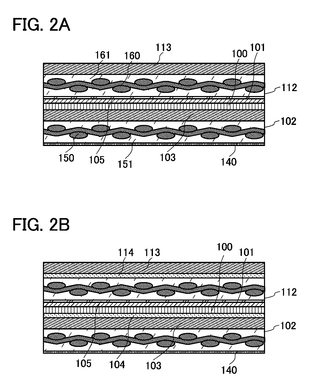
[0148]In this embodiment, another example of a semiconductor device achieving high level of reliability, according to the present invention, is described with reference to FIGS. 22A and 22B. In the structure of this embodiment described below, a common reference numeral refers to the same part or a part having a similar function throughout drawings, in Embodiment 1 and this embodiment, and the description thereof is omitted.

[0149]FIGS. 22A and 22B each illustrate a semiconductor device of this embodiment. In FIG. 22A, the semiconductor integrated circuit 100 is sandwiched between the second impact diffusion layer 103, and the first impact resistance layer 112 and the first impact diffusion layer 113, and the conductive layer 140 is provided on an outer side than the second impact diffusion layer 103 (on the side where the semiconductor integrated circuit 100 is not provided).

[0150]The conductive layer 140 may be provided on an outer side than the first impact diffusion layer 113 (on...

embodiment 3

[0155]In this embodiment, another example of a semiconductor device achieving high level of reliability, according to the present invention, is described with reference to FIGS. 19A and 19B. In the structure of this embodiment described below, a common reference numeral refers to the same part or a part having a similar function throughout drawings in Embodiment 1 and this embodiment, and the description thereof is omitted.

[0156]FIGS. 19A and 19B each illustrate a semiconductor device of this embodiment. In FIG. 19A, the semiconductor integrated circuit 100 is sandwiched between the first impact diffusion layer 113 and the second impact diffusion layer 103, and the conductive layer 140 is provided on an outer side than the second impact diffusion layer 103.

[0157]The conductive layer 140 may be provided on an outer side than the first impact diffusion layer 113 (on the side where the semiconductor integrated circuit 100 is not provided) as long as it covers one of surfaces of the sem...


PUM


Abstract

To reduce defects of a semiconductor device, such as defects in shape and characteristic due to external stress and electrostatic discharge. To provide a highly reliable semiconductor device. In addition, to increase manufacturing yield of a semiconductor device by reducing the above defects in the manufacturing process. The semiconductor device includes a semiconductor integrated circuit sandwiched by impact resistance layers against external stress and an impact diffusion layer diffusing the impact and a conductive layer covering the semiconductor integrated circuit. With the use of the conductive layer covering the semiconductor integrated circuit, electrostatic breakdown (malfunctions of the circuit or damages of a semiconductor element) due to electrostatic discharge of the semiconductor integrated circuit can be prevented.

Description

TECHNICAL FIELD[0001]The present invention relates to a semiconductor device and a method for manufacturing the semiconductor device.BACKGROUND ART[0002]It is important to increase the strength against external stress of a semiconductor integrated circuit chip (also referred to as an IC chip) that is further downsized and thinned.[0003]A variety of methods for strengthening chips have been proposed to increase the strength of chips (see Patent Document 1: Japanese Published Patent Application No. 2006-139802). For example, Patent Document 1 discloses the method in which a chip is sandwiched between reinforcing metal plates, covered with a sealing resin, and hardened.[0004]Further, a semiconductor integrated circuit chip carried to be used has a problem in that it is broken (electrostatic breakdown occurs) due to external electrostatic discharge in being carried, stored, and used, and the measure for the problem is also disclosed (see Patent Document 2: Japanese Published Patent Appl...

Claims


Application Information

Patent Timeline
Patent Type & Authority Applications(United States)
IPC IPC(8): H01L23/28H01L21/56
CPCH01L23/293H01L23/3157H01L2924/12044H01L2924/19041H01L2924/0002H01L21/71H01L2924/00H01L21/02216H01L21/78H01L24/97
Inventor OIKAWA, YOSHIAKIEGUCHI, SHINGOYAMAZAKI, SHUNPEI
Owner SEMICON ENERGY LAB CO LTD
Why Eureka
Try Eureka