Clock control circuit and a semiconductor memory apparatus having the same

a control circuit and memory device technology, applied in the direction of pulse automatic control, pulse technique, digital storage, etc., can solve the problems of deteriorating data output operation stability, affecting the phase of rising and falling clocks, and affecting the stability of data output operation, so as to improve the reliability of output data

Inactive Publication Date: 2009-11-12
SK HYNIX INC
View PDF13 Cites 28 Cited by
  • Summary
  • Abstract
  • Description
  • Claims
  • Application Information

AI Technical Summary

Benefits of technology

[0015]Further, according to the clock control circuit and the semiconductor memory device having the same, the dat...

Problems solved by technology

However, since the data output buffer is not adjacent to the clock generation circuit, the phases of the rising and falling clocks are affected by delay devices existing on a transmission path forwarding to the data output buffer.
In such a case, the stability may deteriorate in a data output operation.
How...

Method used


Image

  • Clock control circuit and a semiconductor memory apparatus having the same
  • Clock control circuit and a semiconductor memory apparatus having the same
  • Clock control circuit and a semiconductor memory apparatus having the same

Examples


Embodiment Construction

.”

BRIEF DESCRIPTION OF THE DRAWINGS

[0017]The above and other aspects, features and other advantages of the subject matter of the present disclosure will be more clearly understood from the following detailed description taken in conjunction with the accompanying drawings, in which:

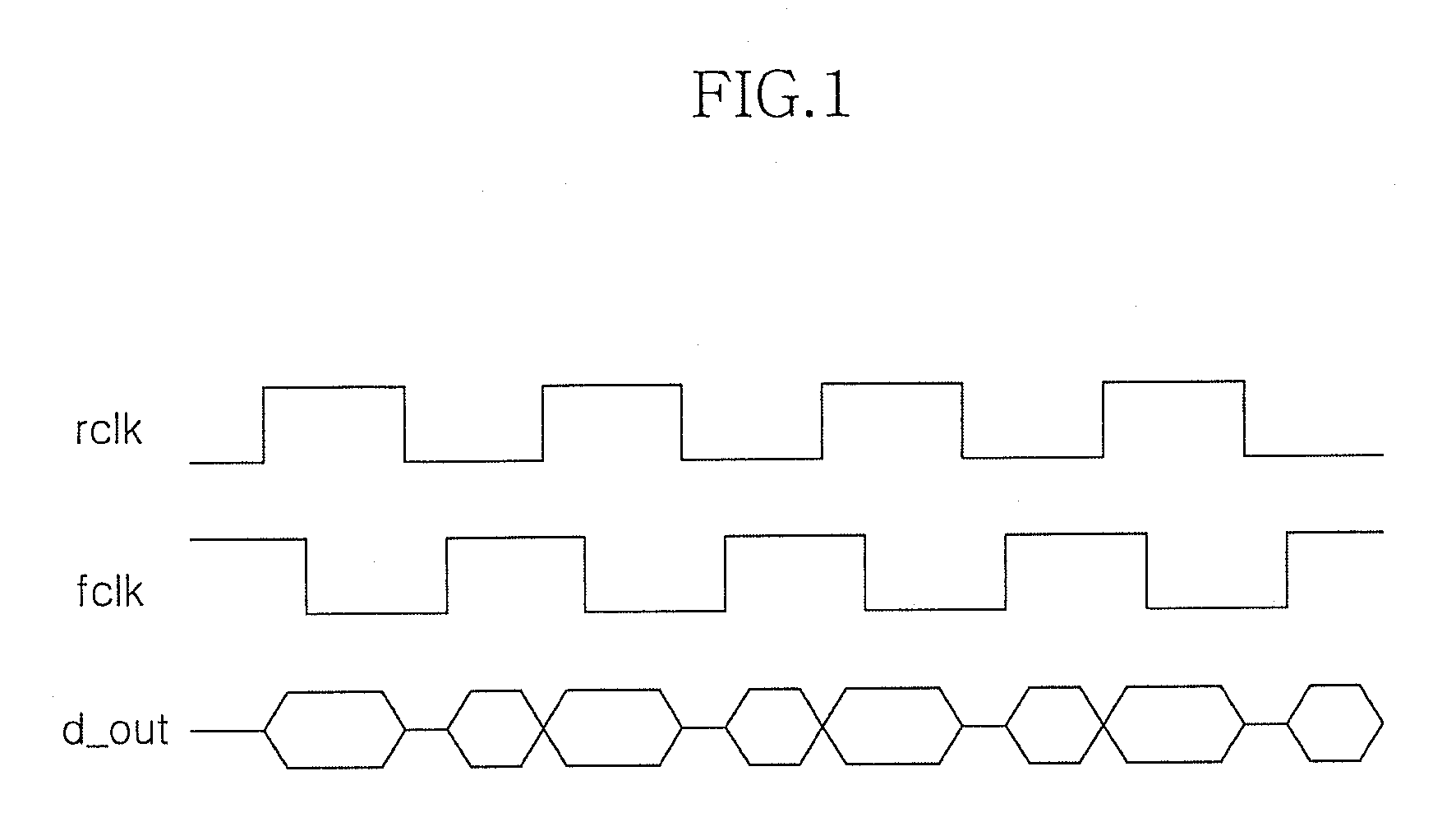
[0018]FIG. 1 is a timing chart illustrating an operation of a conventional semiconductor memory device;

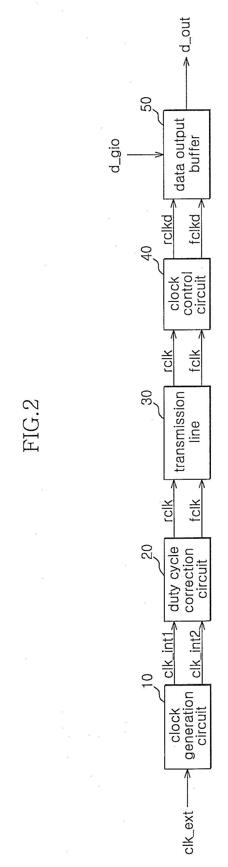
[0019]FIG. 2 is a block diagram illustrating a configuration of a semiconductor memory device in accordance with one embodiment of the present disclosure;

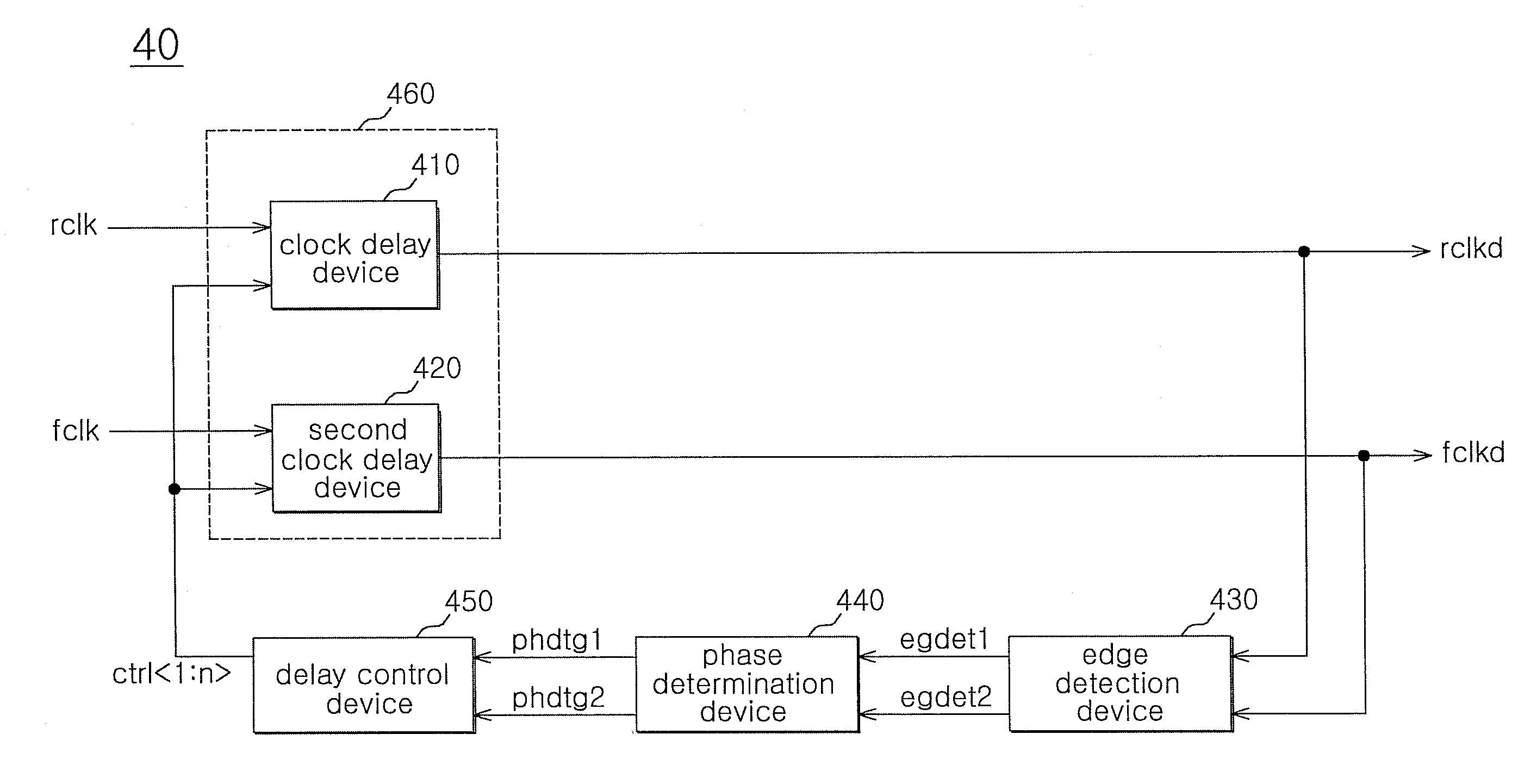
[0020]FIG. 3 is a detailed block diagram illustrating a configuration of the clock control circuit shown in FIG. 2;

[0021]FIG. 4A is a detailed block diagram illustrating a configuration of a first clock delay device shown in FIG. 3;

[0022]FIG. 4B is a detailed block diagram illustrating a configuration of a second clock delay device shown in FIG. 3

[0023]FIG. 5 is a detailed block diagram illustrating a configuration of an edge detection device shown in FI...


PUM


Abstract

A clock control circuit includes a clock delay device, an edge detection device, a phase determination device and a delay control device. The clock delay device generates a delayed rising clock and a delayed falling clock by delaying a rising clock and a falling clock, which are transferred from a clock generation circuit, in response to a control signal, and to transfer the delayed rising clock and the delayed falling clock to a data output buffer. The edge detection device detects a difference between an edge timing of the delayed rising clock and an edge timing of the delayed falling clock to generate edge detection signals. The phase determination device detects a duty ratio of each of the edge detection signals to generate phase determination signals. The delay control device generates the control signal in response to the phase determination signals.

Description

CROSS-REFERENCES TO RELATED APPLICATION[0001]The present application claims priority under 35 U.S.C. 119(a) to Korean application number 10-2008-0043657, filed on May 9, 2008, in the Korean Patent Office, which is incorporated by reference in its entirety as if set forth herein in full.BACKGROUND OF THE INVENTION[0002]1. Technical Field[0003]The present invention relates to a semiconductor memory device, and more particularly to a clock control circuit of a semiconductor memory device.[0004]2. Related Art[0005]In general, a semiconductor memory device includes a clock generation circuit such as a delay locked loop (DLL) circuit or a phase locked loop (PLL) circuit to generate an internal clock having a phase advanced by a predetermined time as compared with that of an external clock. In a semiconductor memory device such as a double data rate synchronous dynamic random access memory (DDR SDRAM), the internal clock output from the clock generation circuit includes a rising clock and ...

Claims


Application Information

Patent Timeline
IPC IPC(8): H03L7/06H03L7/00
CPCH03K5/1254H03L7/0814H03K2005/00052H03K5/13G11C11/407G11C11/4076
Inventor KIM, KWAN DONG
Owner SK HYNIX INC
Why Eureka
Try Eureka