Apparatus for etching semiconductor wafers

a technology for etching apparatuses and semiconductor wafers, which is applied in the direction of manufacturing tools, mechanical apparatus, chucks, etc., can solve the problems of reactants and byproducts that can undetectable condensate, adversely affect the surface uniformity of substrates, and etchants and/or byproducts that are prone to condensation, so as to prevent the deflection of substrates

Active Publication Date: 2009-11-19
APPLIED MATERIALS INC
View PDF8 Cites 373 Cited by
  • Summary
  • Abstract
  • Description
  • Claims
  • Application Information

AI Technical Summary

Benefits of technology

[0004]Embodiments of the present invention pertain to wafer pedestal and semiconductor apparatus thereof that provide benefits over previously known wafer chucks by configuring the sealing band toward the center of the pedestal and distant from the edge of the pedestal. In embodiments, the sealing band may be configured between the chucking openings and purge openings of the pedestal. The sealing band may be disposed

Problems solved by technology

The reactants and byproducts may undesirably condense, forming particles within the etch processing chamber.
The particles and/or byproducts formed within the processing chamber may adversely affect surface uniformity of the substrates.
The etchants and/or byproducts are prone to condensing on the sealing ba

Method used


Image

  • Apparatus for etching semiconductor wafers
  • Apparatus for etching semiconductor wafers
  • Apparatus for etching semiconductor wafers

Examples


Embodiment Construction

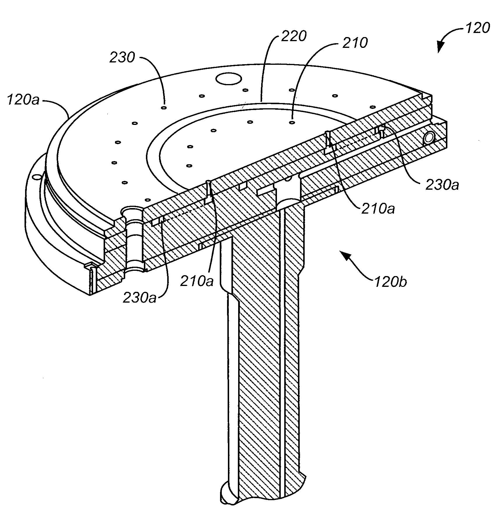
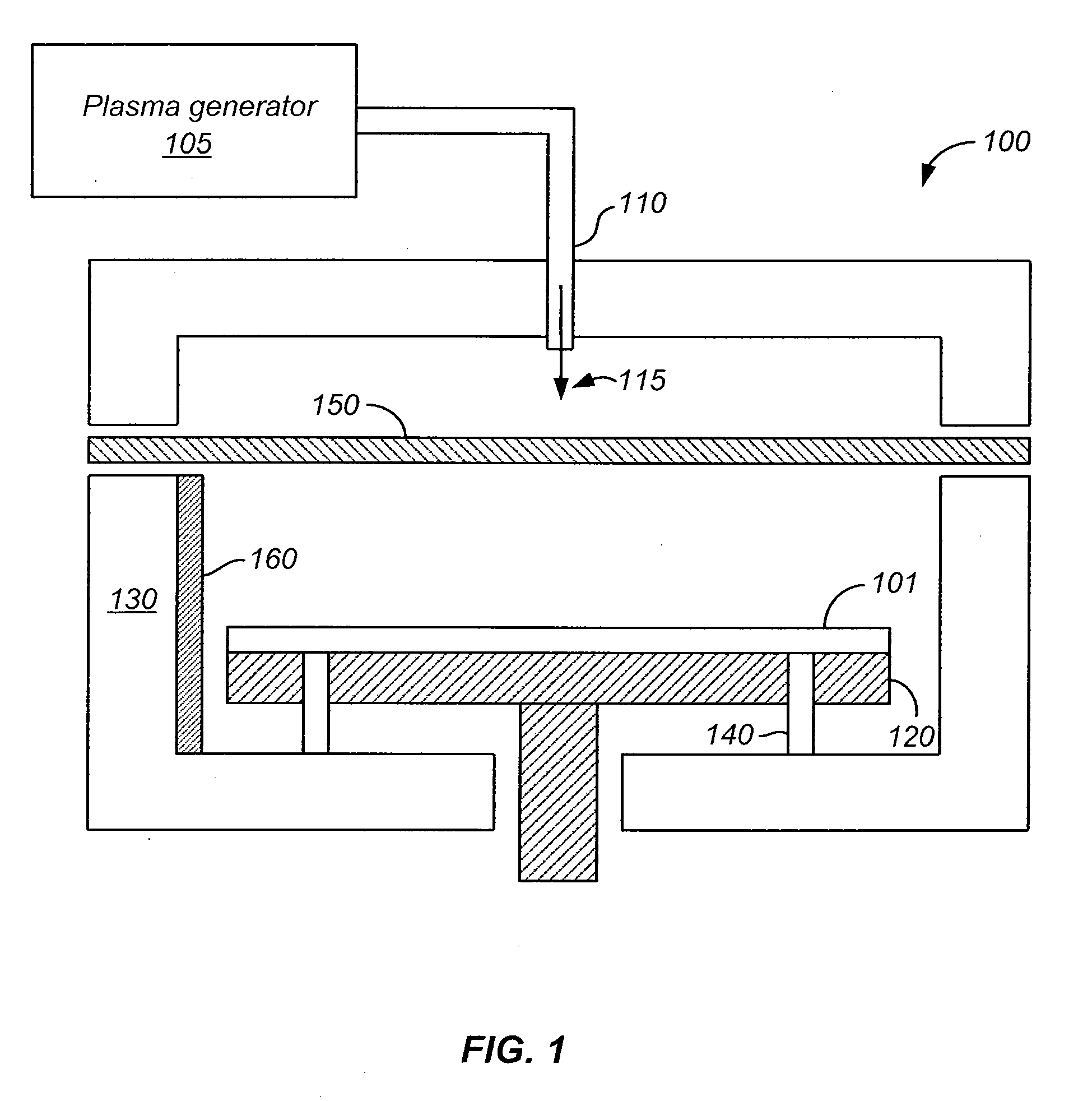
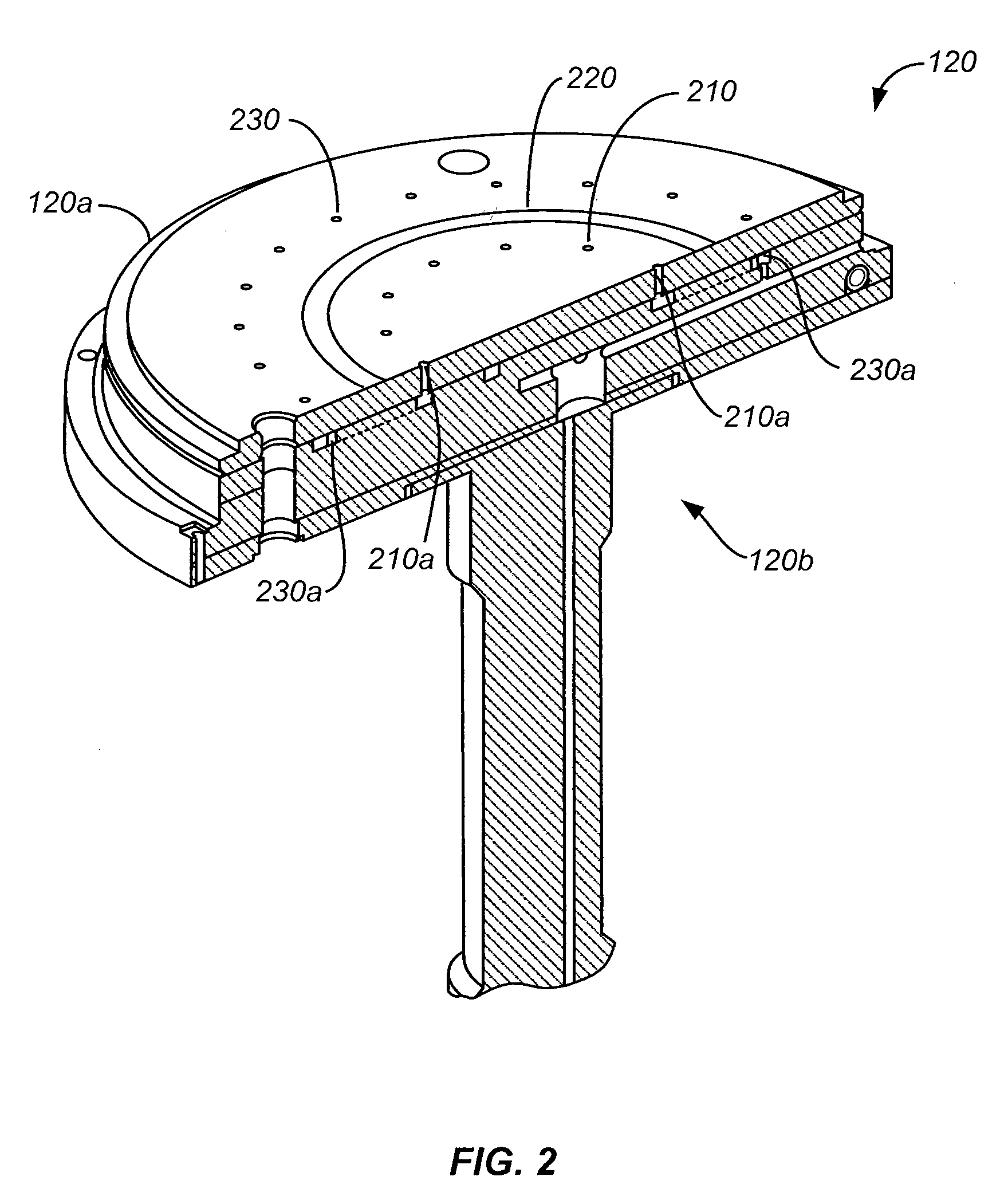
[0014]The present invention relates to wafer pedestal and semiconductor apparatus for etching, cleaning or precleaning substrates, such as silicon wafers, liquid crystal display substrates, solar panel substrates, and others. In embodiments, the wafer pedestal can be used in a deposition chamber such as a chemical vapor deposition (CVD) chamber. A wafer pedestal of a semiconductor apparatus is capable of supporting a substrate. The wafer pedestal may include a pedestal having at least one purge opening configured to flow a purge gas and at least one chucking opening configured to chuck the substrate over the pedestal. The pedestal may also include a sealing-band disposed between the at least one purge opening and the at least one chucking opening. The sealing band is configured to support the substrate. The configuration of the sealing band can desirably prevent the condensation of reactants and / or byproducts on the sealing band during sublimation. Additionally, the location of the ...


PUM

PropertyMeasurementUnit
Lengthaaaaaaaaaa
Lengthaaaaaaaaaa
Pressureaaaaaaaaaa

Abstract

A wafer pedestal of a semiconductor apparatus is provided. The wafer pedestal is capable of supporting a substrate. The wafer pedestal includes a pedestal having at least one purge opening configured to flow a purge gas and at least one chucking opening configured to chuck the substrate over the pedestal. The pedestal includes a sealing band disposed between the at least one purge opening and the at least one chucking opening. The sealing band is configured to support the substrate.

Description

FIELD OF THE INVENTION[0001]The present invention relates to components and apparatus for semiconductor manufacturing. More particularly, the present invention relates to wafer pedestal and semiconductor apparatuses thereof.BACKGROUND OF THE INVENTION[0002]When processing silicon wafers, a good product requires surface uniformity. Achieving surface uniformity, etch, clean and / or preclean processes are implemented to remove semiconductor materials, dielectric materials and / or metallic materials. Usually, an etching process uses various reactants and / or plasmas to remove semiconductor materials and generated byproducts. The reactants and byproducts may undesirably condense, forming particles within the etch processing chamber. The particles and / or byproducts formed within the processing chamber may adversely affect surface uniformity of the substrates.[0003]For a conventional etch apparatus, a pedestal is configured to support a wafer within an etch chamber for an etch process. The pe...

Claims


Application Information

Patent Timeline
IPC IPC(8): H01L21/3065
CPCH01L21/67126Y10T279/23H01L21/6838
Inventor LUBOMIRSKY, DMITRYTAN, TIEN FAKTSUEI, LUN
Owner APPLIED MATERIALS INC
Why Eureka
Try Eureka