Display device

a display device and display technology, applied in the direction of discharge tube luminescnet screens, instruments, and semiconductor/solid-state device details, can solve the problems of degrading display quality, deviation in sampling timing, and deviation in sampling timing, and achieve the effect of increasing screen siz

Inactive Publication Date: 2009-11-19
SONY CORP
View PDF4 Cites 27 Cited by
  • Summary
  • Abstract
  • Description
  • Claims
  • Application Information

AI Technical Summary

Benefits of technology

[0036]The present invention permits easy design of the sampling timing for various types of display devices including self-luminous ones such as organic EL display devices and optical modulation o

Problems solved by technology

As a result, a large screen leads to a large signal delay in the control lines running in the row direction, readily resulting in a deviation in sampling timing particularly between pixels in the same row close to and far from the vertical drive circuit adapted to control the control lines.
A large deviation in sampling timing gives rise to degraded display quality due to sampling of the video signal at a wrong level unless corrected, for example, by securing a large margin for variat

Method used


Image

  • Display device
  • Display device
  • Display device

Examples


Embodiment Construction

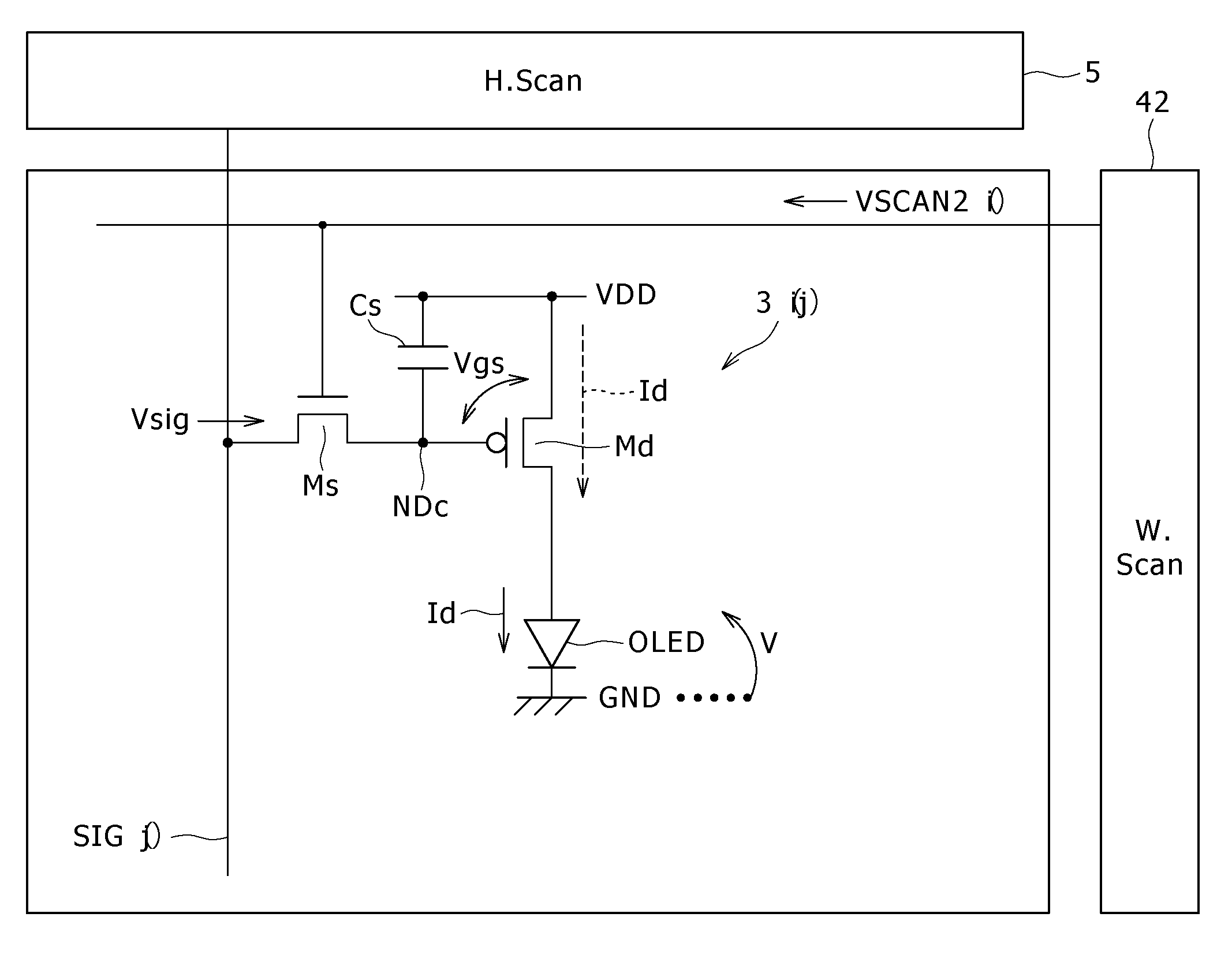
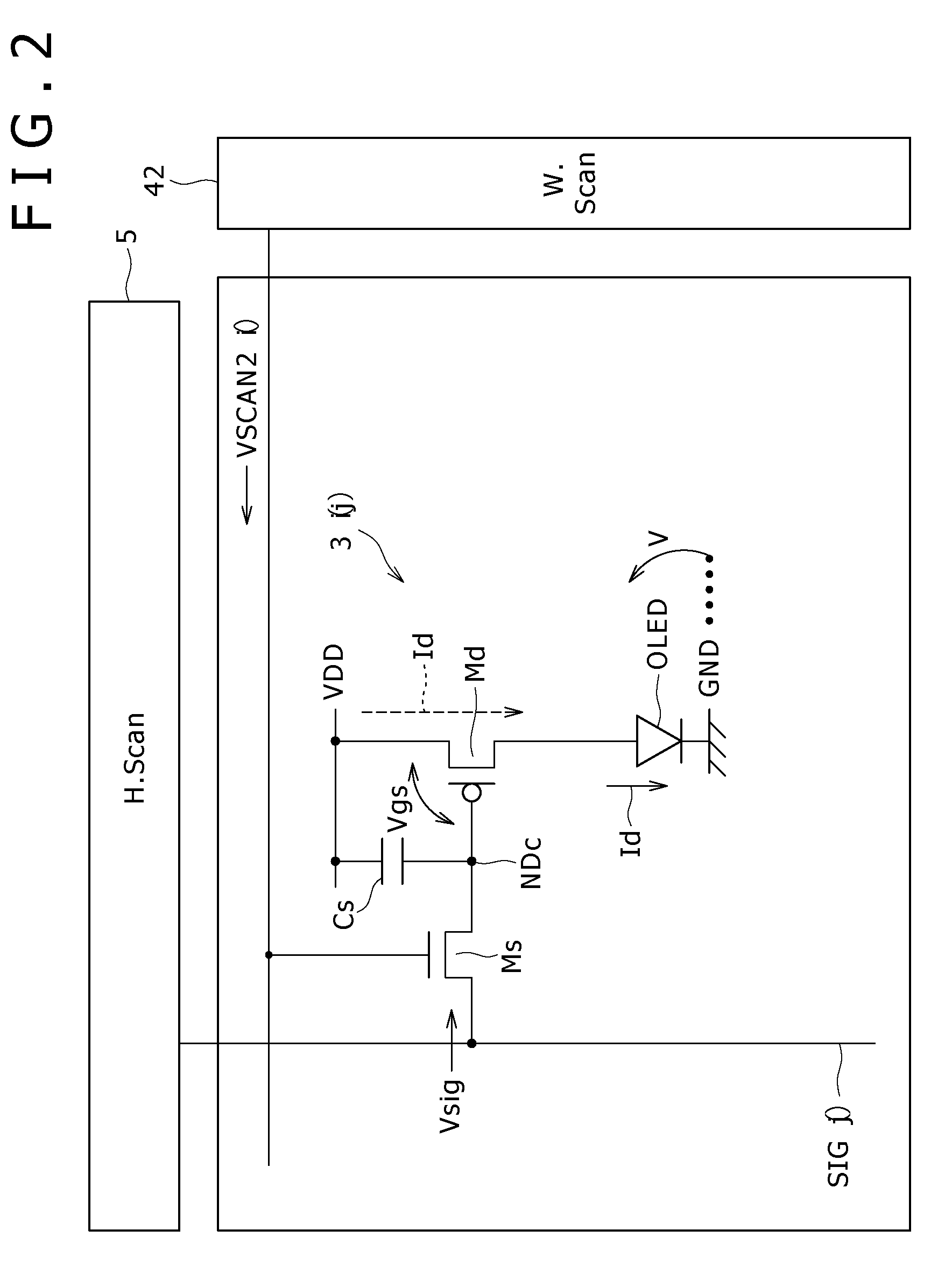
[0051]The present invention may be applied to liquid crystal and other display devices. However, embodiments of the present invention will be described below with reference to the accompanying drawings taking, as an example, a case in which the present invention is applied to an organic EL display device.

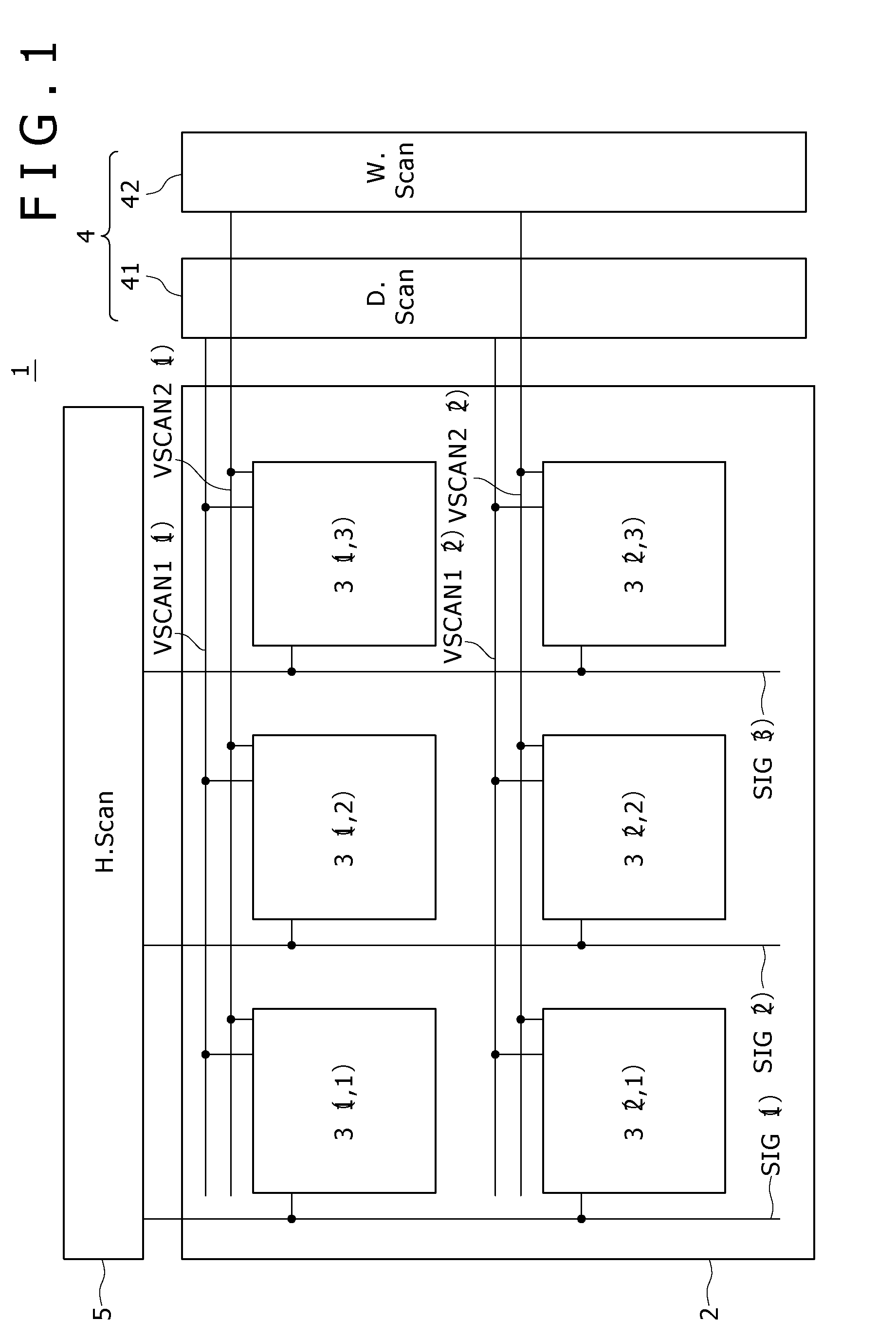
[0052]FIG. 1 is a diagram illustrating the major components of an organic EL display device according to an embodiment of the present invention.

[0053]An organic EL display device 1 illustrated in FIG. 1 includes a pixel array 2 and drive circuit. The pixel array 2 has a plurality of pixel circuits 3(i,j) arranged in a matrix form. The drive circuit drives the pixel array 2 and includes a vertical drive circuit (V scanner) 4 and horizontal drive circuit (H scanner or H. Scan).

[0054]The plurality of V scanners 4 are provided depending on the configuration of the pixel circuits 3. Here, the V scanner 4 includes a horizontal pixel line drive circuit (Drive Scan) 41 and write signal scan...


PUM

PropertyMeasurementUnit
Lengthaaaaaaaaaa
Electrical resistanceaaaaaaaaaa

Abstract

A display device includes: a pixel array having a plurality of pixels arranged in a matrix form, each of the pixels including a sampling transistor configured to sample a data potential from a video signal line which is insulated from and intersects a control line in response to the change in potential of the control line, and a light-emitting element configured to emit light at the brightness commensurate with the magnitude of the post-sampling data potential.

Description

BACKGROUND OF THE INVENTION[0001]1. Field of the Invention[0002]The present invention relates to a display device which includes a pixel array having a plurality of pixels arranged in a matrix form and wirings, common to the plurality of pixels and disposed in two directions, intersecting with each other in the pixels. More specifically, the present invention relates to a wiring forming technique for minimizing the number of wirings disposed in the two directions and bringing the resistances thereof close to each other to the extent possible.[0003]2. Description of the Related Art[0004]Some display devices use electro-optical elements whose brightness changes with change in voltage applied thereto or current flowing therethrough. For example, a liquid crystal display element is a typical example of an electro-optical element whose brightness changes with change in voltage applied thereto. A display device using such elements is called a “liquid crystal display device.”[0005]On the o...

Claims


Application Information

Patent Timeline
IPC IPC(8): G09G3/30H01J1/53H05B44/00
CPCG09G3/3233G09G2300/0426G09G2300/0465G09G2300/0819H05B33/08G09G2300/0866G09G2320/0223H01L27/3276G09G2300/0842C22C38/22H05B45/00Y02B20/30H10K59/1216H10K59/131H10K50/805H10K59/123H01L23/53214
Inventor YAMAMOTO, TETSUROUCHINO, KATSUHIDE
Owner SONY CORP
Why Eureka
Try Eureka