Method for Producing Printing Stencils, Particularly for Screen Printing Methods, and a Stencil Device

Inactive Publication Date: 2009-11-26
ROBERT BOSCH GMBH
View PDF3 Cites 5 Cited by
  • Summary
  • Abstract
  • Description
  • Claims
  • Application Information

AI Technical Summary

Benefits of technology

[0005]One stencil device according to the present invention, having a printing stencil, particularly for use in filling at least one contact hole formed in a printed-circuit board, is able to be produced in the same working process as the contact hole, particularly in a punching process. The holes on the

Problems solved by technology

It is disadvantageous, in this instance, that manufacturing tolerances of stamped vias in ceramic tape, for example, as well as tolerances that

Method used


Image

  • Method for Producing Printing Stencils, Particularly for Screen Printing Methods, and a Stencil Device
  • Method for Producing Printing Stencils, Particularly for Screen Printing Methods, and a Stencil Device
  • Method for Producing Printing Stencils, Particularly for Screen Printing Methods, and a Stencil Device

Examples


Embodiment Construction

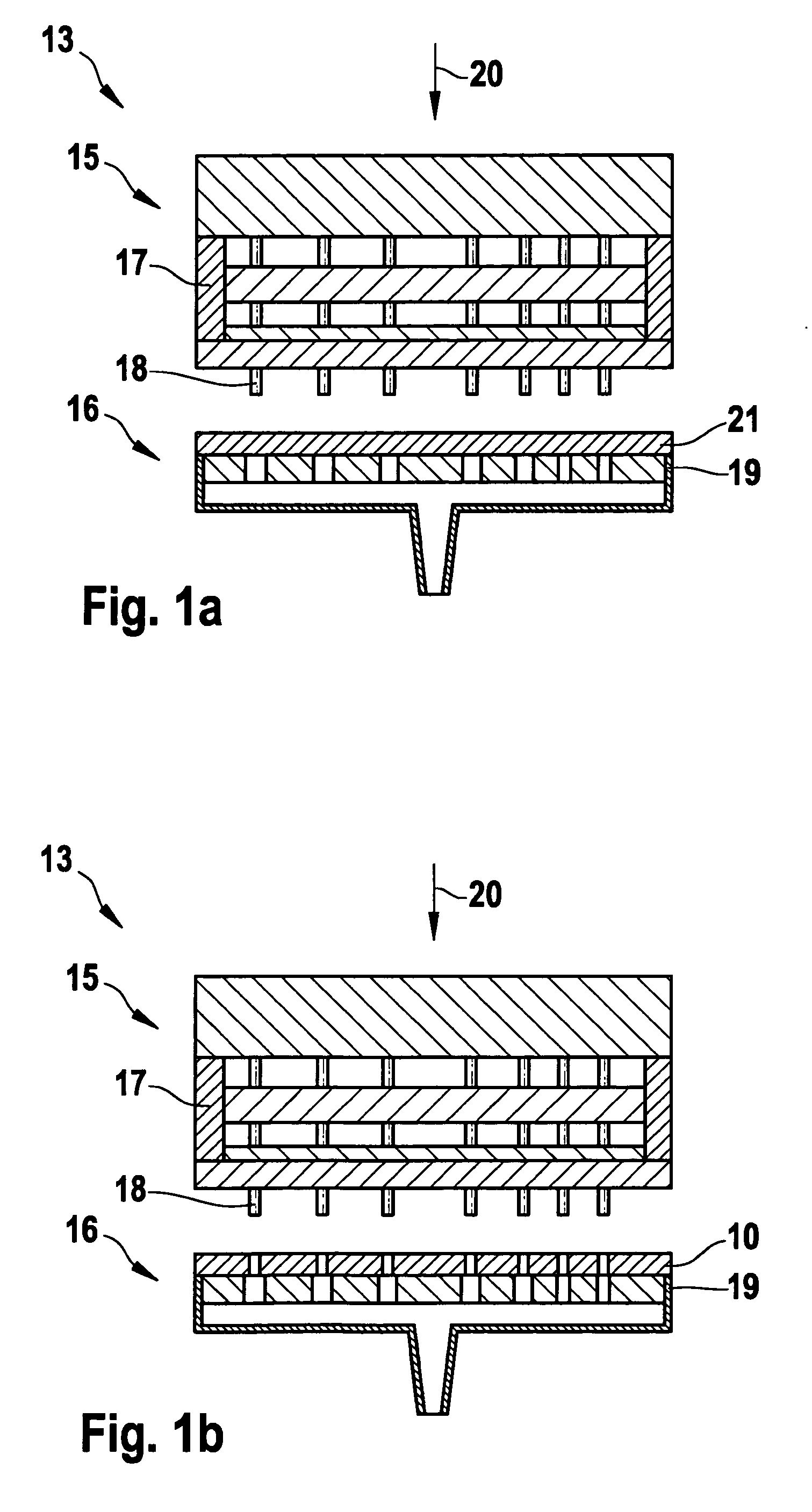
[0009]In FIGS. 1a and 1b, a production process of a stencil 10, according to the present invention, using a stamping tool 13, is shown schematically. Stamping tool 13 includes an upper part 15 and a lower part 16. Upper part 15 includes a punch 17 as well as punching needles 18, which are able to be moved back and forth in punching direction 20, and which punch an element arranged on a cutting die 19 according to a specified cutting pattern. A still unprocessed stencil blank 21 is clamped between upper part 15 and lower part 16 in FIG. 1a. In FIG. 1b, stencil blank 21 has been punched, and is able to be used as a stencil 10, for instance, in a via-fill process.

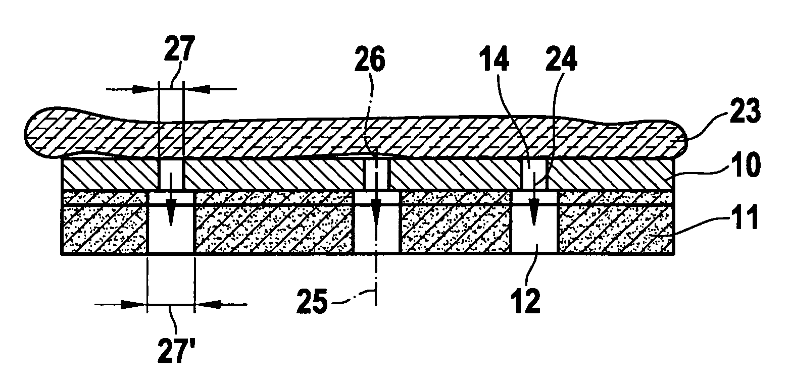
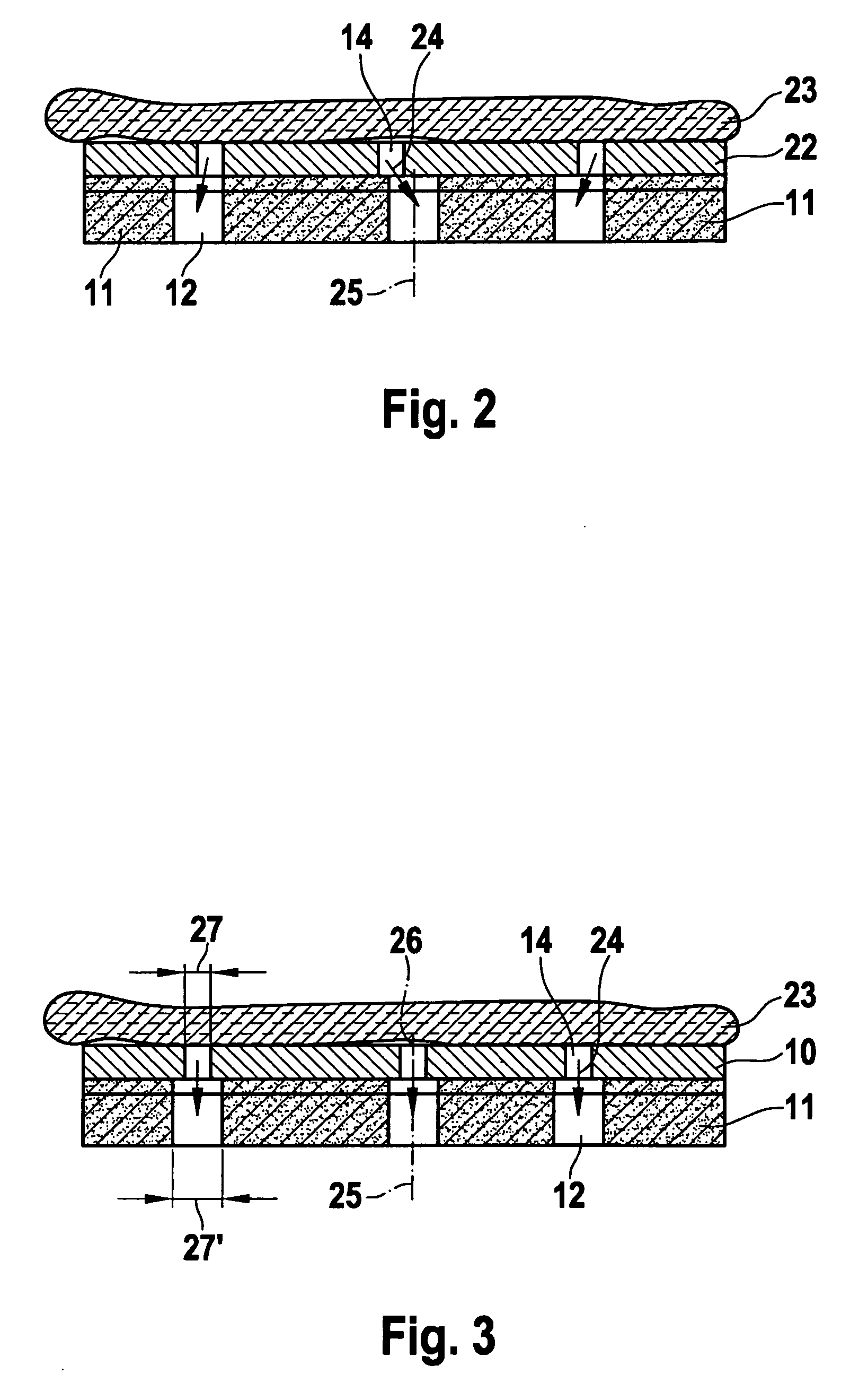
[0010]FIG. 2 shows a filling process of vias in a via-fill process, using a stencil 22, produced according to the related art, for example, by laser. Printed-circuit board 11 is formed particularly of a ceramic substrate or ceramic tape, and has contact holes 12 in the form of blind holes or vias. The pattern artwork of lasere...


PUM


Abstract

A method for producing printing stencils, especially for screen printing methods, and particularly those for use in filling at least one contact hole formed in a printed-circuit board, a pattern artwork being reproduced on the stencil, which corresponds to an arrangement of contact holes on the printed-circuit board. It is provided that the pattern artwork reproduced on the stencil be produced in the same working process, especially a punching process, using a cluster punching tool, as the at least one contact hole on the printed-circuit board. Also, a stencil device is provided.

Description

BACKGROUND INFORMATION[0001]Integrated electronic components usually include at least one printed-circuit board, on whose front side electronic power components are situated. It is known, particularly when using a printed-circuit board material made of plastic or ceramic foils, that one may bore or punch contact holes or through contacting into the printed-circuit boards, whose diameters tend to be in the p range and which are designated as μ vias (or microvias). The vias are provided on the one hand to support vertical heat transport of the electronic power components situated on the front side of the mounting board to the back side. Such thermal through contacting (or thermal vias) are developed as small holes or blind holes, which may be generated using laser technology or mechanically, using a microbore or punching needle, and used for heat conduction. On the other hand, the through contacting may be provided for the electrical connection of the components situated on the front ...

Claims


Application Information

Patent Timeline
IPC IPC(8): B05C17/08B41M1/12
CPCB41C1/14B41F15/34B41F15/36B41P2215/12H05K3/4061H05K3/005H05K3/1225H05K3/4053H05K1/0306
Inventor MAIHOEFER, BERNDMEIER, ANDREASLEVERKOEHNE, MARKSPEH, ULRICHLIEB, GUNTHERDIRSCHERL, ALEXANDRASCHAEFER, JOERG
Owner ROBERT BOSCH GMBH
Why Eureka
Try Eureka