Nonvolatile memory device

a memory device and non-volatile technology, applied in static storage, digital storage, instruments, etc., can solve the problems of program time increase, disadvantageous non-volatile flash memory, etc., and achieve the effect of reducing the amount of time to pre-charg

Inactive Publication Date: 2009-11-26
SK HYNIX INC
View PDF2 Cites 11 Cited by
  • Summary
  • Abstract
  • Description
  • Claims
  • Application Information

AI Technical Summary

Benefits of technology

[0018]The present invention is directed toward a nonvolatile memory device in which precharge and discharge are possible across a bit line so as to reduce the amount of time to precharge and discharge the bit line of the nonvolatile memory device.

Problems solved by technology

In general, NOR type flash memory is disadvantageous in regard to high integration because of high current consumption, but is advantageous in regard to high speed.
However, when a step voltage is set to be low, a program time increases.

Method used


Image

  • Nonvolatile memory device
  • Nonvolatile memory device
  • Nonvolatile memory device

Examples


Embodiment Construction

[0031]A specific embodiment according to the present invention will be described with reference to the accompanying drawings. However, the present invention is not limited to the disclosed embodiment, but may be implemented in various ways. The embodiment is provided to complete the disclosure of the present invention and to allow those having ordinary skill in the art to understand the present invention. The present invention is defined by the scope of the claims.

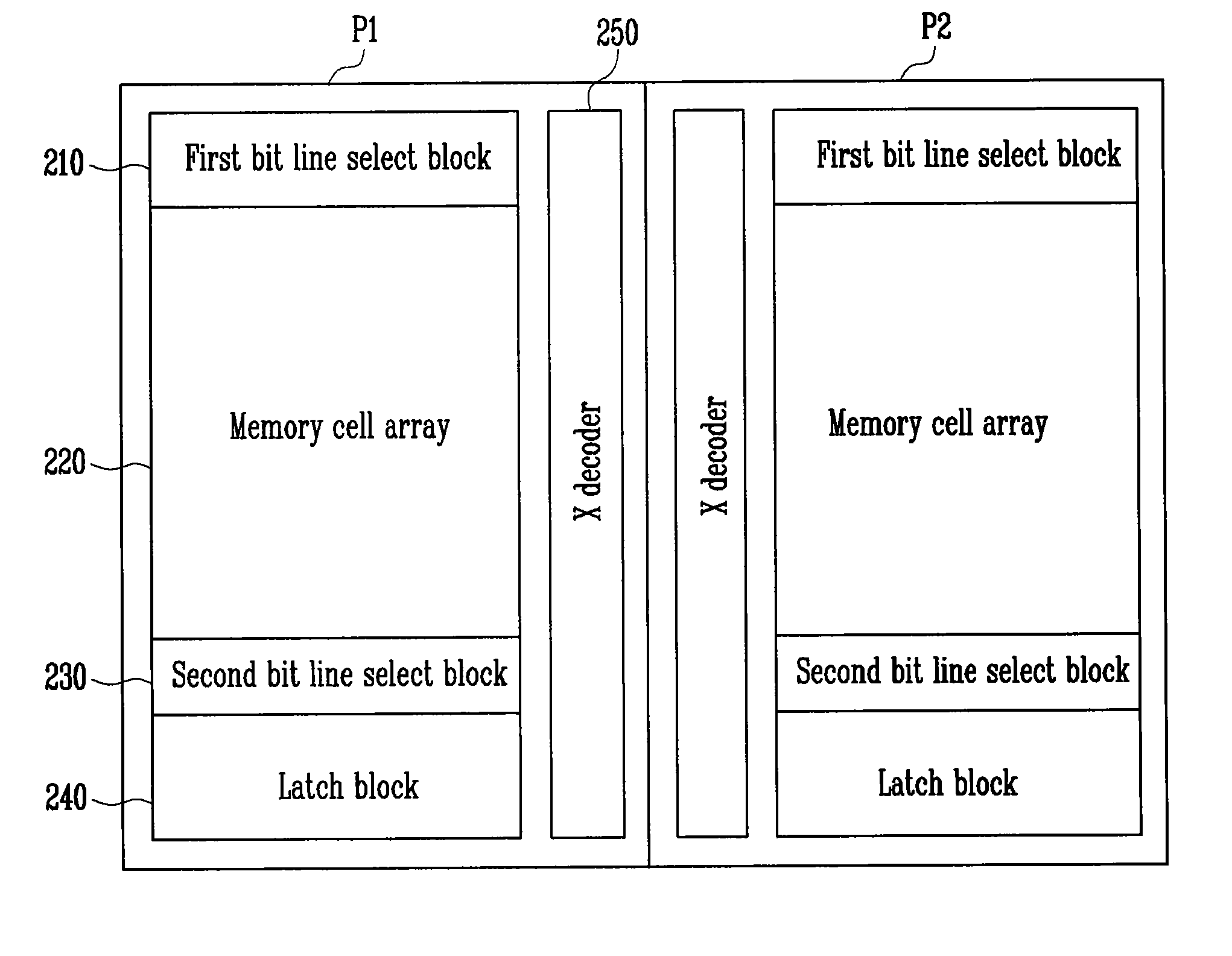
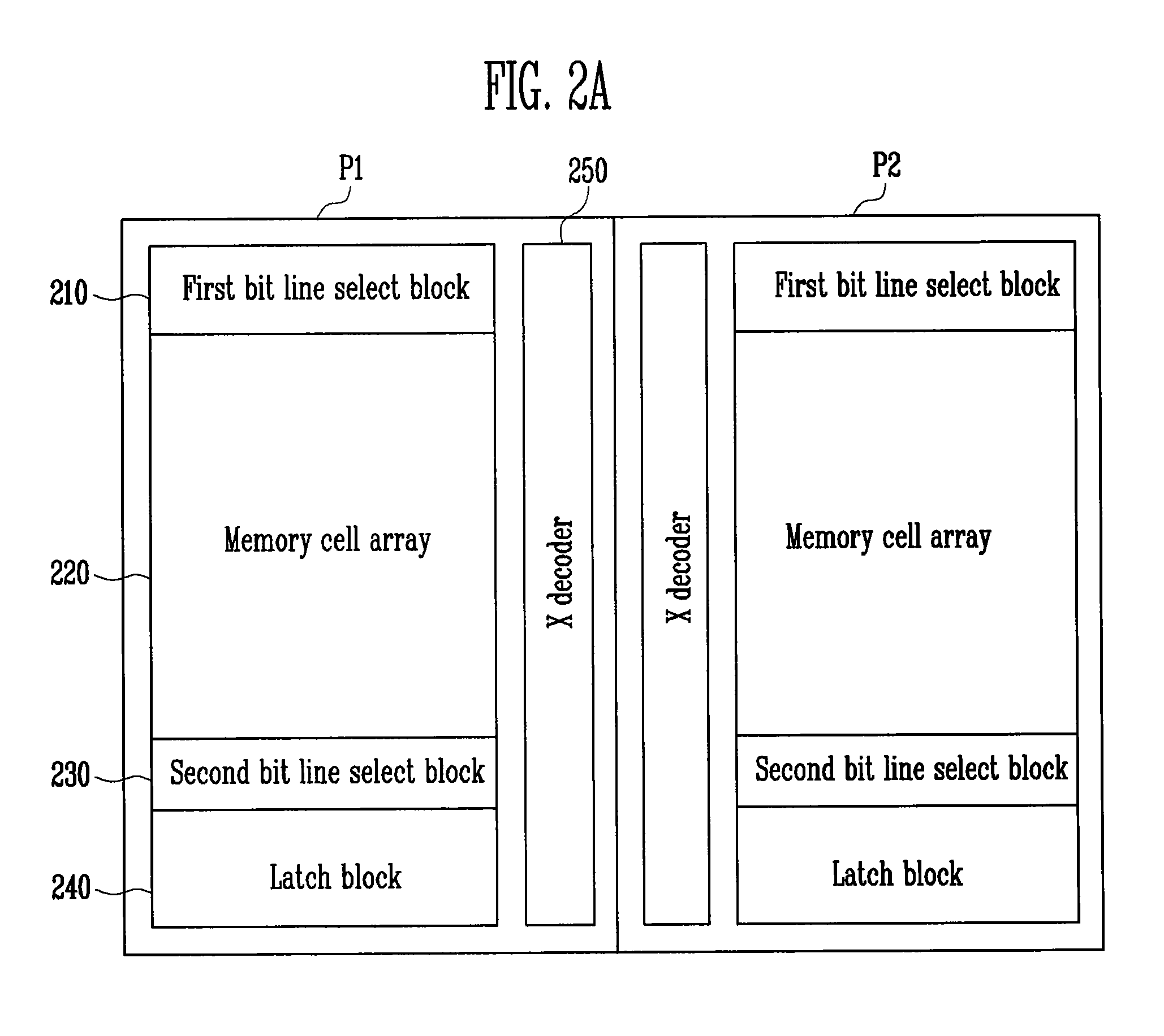
[0032]FIG. 2A is a block diagram of a nonvolatile memory device in accordance with an embodiment of the present invention. FIG. 2B is a detailed circuit diagram of FIG. 2A.

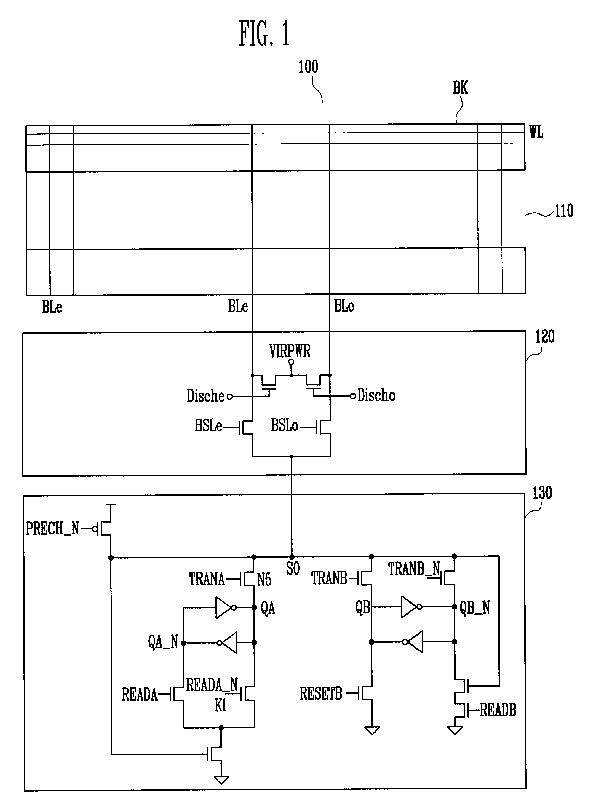
[0033]Referring to FIGS. 2A and 2B, a nonvolatile memory device in accordance with an embodiment of the present invention includes first and second planes P1, P2. Each of the planes includes a first bit line select block 210, a memory cell array 220, a second bit line select block 230, and a latch block 240.

[0034]The memory cell array 220 includes memory...


PUM


Abstract

A nonvolatile memory device includes a page buffer circuit. The page buffer circuit includes a memory cell area, a first bit line select unit, and a second bit line select unit. A plurality of memory cells of the memory cell area is connected by bit lines and word lines. The first bit line select unit i s connected to one or more bit lines of the memory cell area and is configured to precharge or discharge a selected bit line in response to a control signal. The second bit line select unit is connected to the same bit line as the first bit line select unit and is configured to precharge or discharge the selected bit line simultaneously with the first bit line select unit.

Description

CROSS-REFERENCES TO RELATED APPLICATIONS[0001]The present application claims priority to Korean patent application number 10-2008-0046597, filed on May 20, 2008, which is incorporated by reference in its entirety.BACKGROUND OF THE INVENTION[0002]The present invention relates to nonvolatile memory devices and, more particularly, to nonvolatile memory devices which can reduce the amount of time required to precharge and discharge a bit line.[0003]A semiconductor memory device is a memory device that is able to store data and read stored data. Semiconductor memory devices include volatile memory, which loses stored data when power is off, and nonvolatile memory, which retains stored data although power is off. Flash memory electrically erases data of cells in a group, and has been widely used in computers, memory cards, etc.[0004]Flash memory is divided into a NOR type and a NAND type according to bit lines of a cell and the connection status of the bit lines. NOR type flash memory has...

Claims


Application Information

Patent Timeline
Patent Type & Authority Applications(United States)
IPC IPC(8): G11C16/06G11C7/00
CPCG11C7/1039G11C16/24G11C7/12G11C5/063G11C7/18G11C16/10G11C16/26
Inventor PARK, SE CHUNKIM, DUCK JUYANG, CHANG WON
Owner SK HYNIX INC
Why Eureka
Try Eureka