Method and correction apparatus for correcting process proximity effect and computer program product

a technology of proximity effect and process, applied in the field of graphic processing method for design data of semiconductor integrated circuit devices, can solve the problems of insufficient accuracy, becoming increasingly difficult to obtain finished patterns (patterns formed on a substrate) faithful to design data,

Inactive Publication Date: 2009-11-26
KK TOSHIBA
View PDF8 Cites 3 Cited by
  • Summary
  • Abstract
  • Description
  • Claims
  • Application Information

AI Technical Summary

Problems solved by technology

As a semiconductor integrated circuit device advance in fine patterning, it becomes increasingly difficult to obtain finished patterns (patterns formed on a substrate) faithful to design data.
However, these methods do not ensure sufficient accuracy.

Method used


Image

  • Method and correction apparatus for correcting process proximity effect and computer program product
  • Method and correction apparatus for correcting process proximity effect and computer program product
  • Method and correction apparatus for correcting process proximity effect and computer program product

Examples


first embodiment

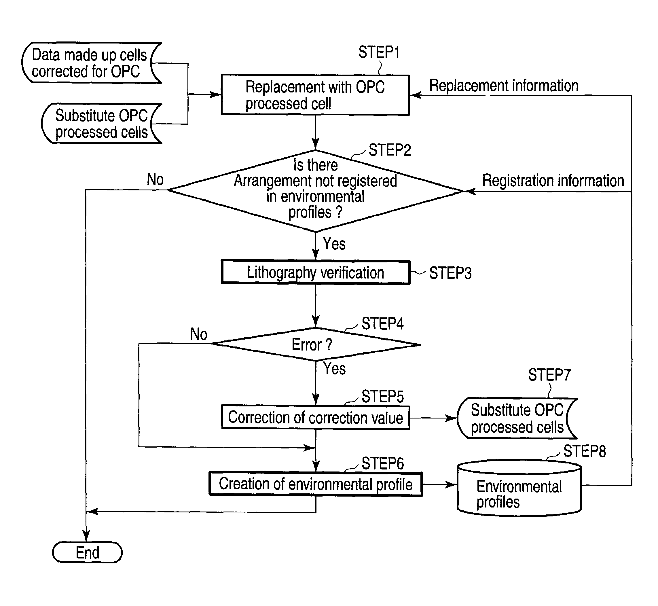
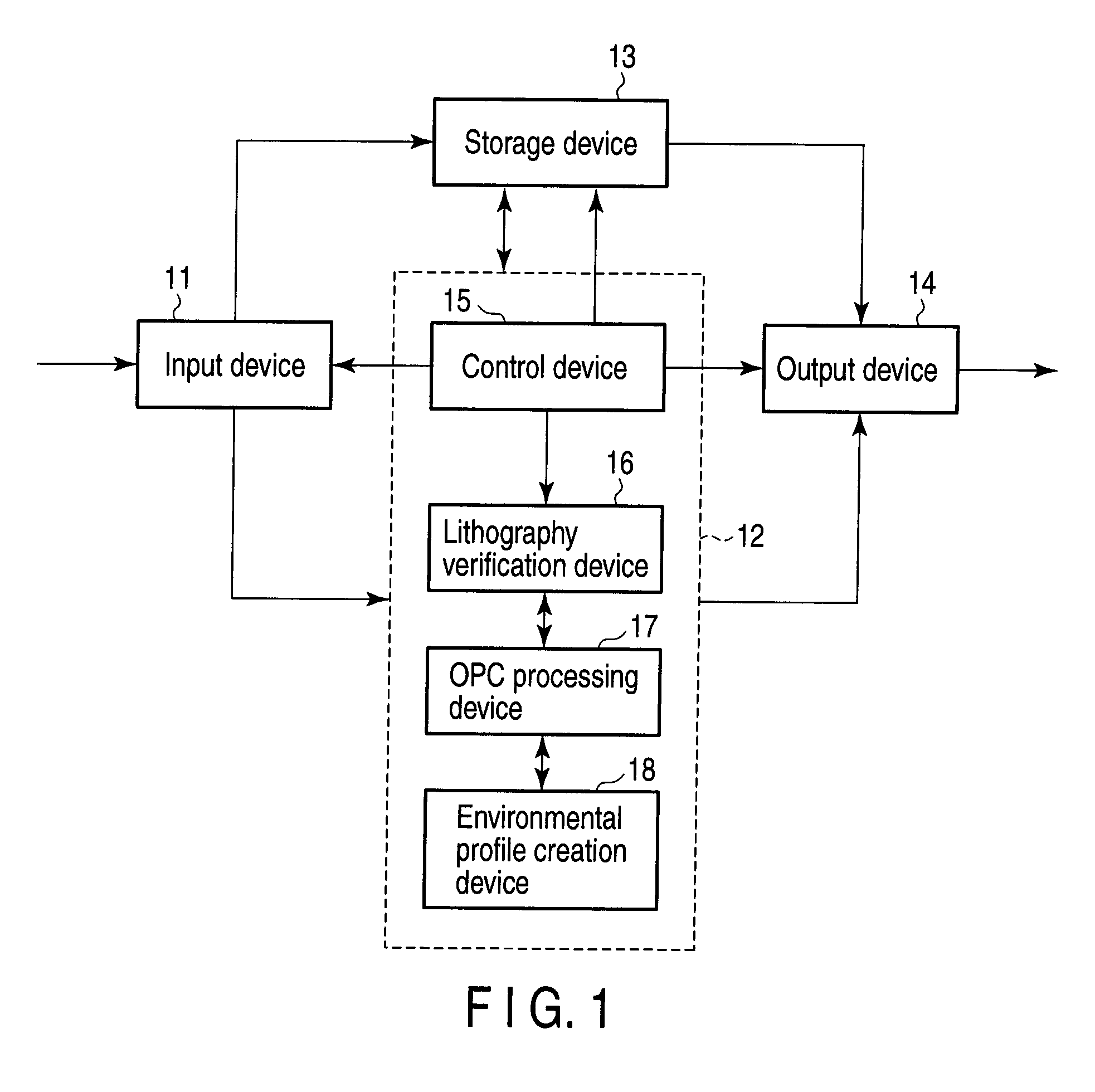
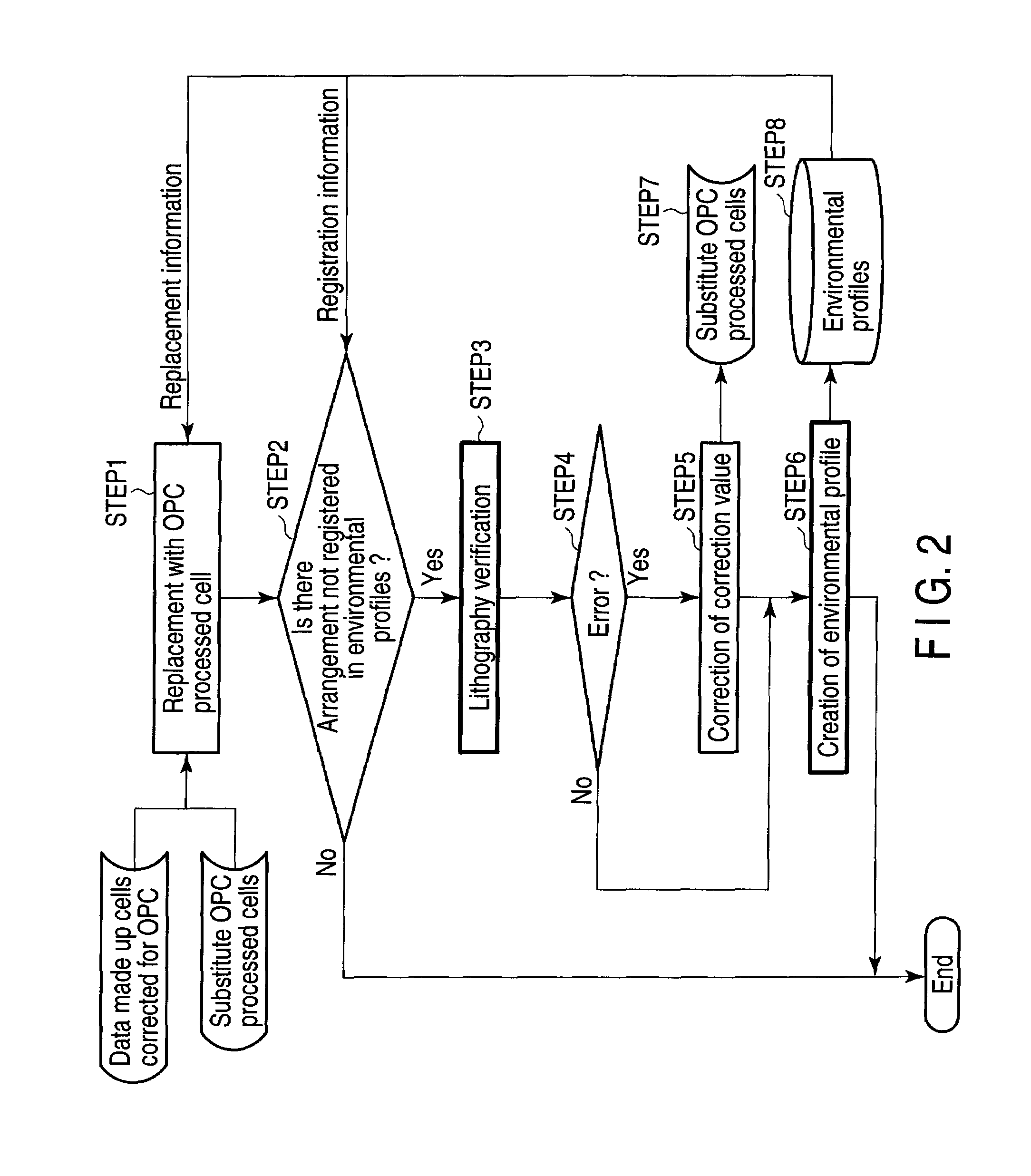
[0052]FIG. 1 is a schematic block diagram of a process proximity effect correction apparatus according to a first embodiment.

[0053]The correction apparatus comprises an input device 11, such as a console or a keyboard, which inputs design data of a semiconductor integrated circuit device, a processing device 12 which performs various processes and control to correct the process proximity effect, a storage device 13 which is comprised of a semiconductor memory or a hard disk driver to store the design data, the results of lithography verification, the results of correction of correction values, created environmental profiles, etc., and an output device 14, such as a monitor or a printer.

[0054]The processing device 12 includes a control device 15, a lithography verification device 16, an optical proximity effect correction (OPC) processing device 17, and an environmental profile creation device 18. The control device 15 controls the operations of the input device 11, the storage devic...

second embodiment

[0109]FIG. 21 is a flowchart illustrating a process proximity correction method according to a second embodiment and another method of lithography verification.

[0110]FIG. 22 is a plan view illustrating the concept of the lithography verification method shown in FIG. 21.

[0111]FIG. 23 is a flowchart illustrating redivision of an area in the lithography verification method shown in FIG. 21.

[0112]FIGS. 24A and 24B are pattern plan views illustrating the arrangement of divisional areas in the lithography verification method shown in FIG. 23.

[0113]FIG. 25 is a pattern plan view illustrating the step of combining the divisional areas in the lithography verification method shown in FIG. 23.

[0114]FIG. 26 is a pattern plan view illustrating the step of creating a reverification area in the lithography verification method shown in FIG. 23.

[0115]FIG. 27 is a pattern plan view illustrating the redivision step in the lithography verification method shown in FIG. 23.

[0116]In the second embodiment,...

third embodiment

[0123]FIG. 28 is a flowchart illustrating a process proximity correction method according to a third embodiment and another concept of the lithography verification method shown in FIG. 21.

[0124]FIG. 29 is a flowchart illustrating the lithography verification method shown in FIG. 28.

[0125]FIGS. 30A and 30B are pattern plan views illustrating the arrangement of cells in the lithography verification method shown in FIG. 29.

[0126]FIG. 31 is a pattern plan view illustrating the step of combining the divisional areas in the lithography verification method shown in FIG. 29.

[0127]FIG. 32 is a pattern plan view illustrating the step of creating a reverification area in the lithography verification method shown in FIG. 29.

[0128]FIG. 33 is a pattern plan view illustrating the redivision step in the lithography verification method shown in FIG. 29.

[0129]The third embodiment adopts a dividing method in the STEP 72 of dividing the area defined by the input data, in which the dividing method divid...


PUM

PropertyMeasurementUnit
optical radiusaaaaaaaaaa
proximity effectaaaaaaaaaa
areaaaaaaaaaaa

Abstract

A process proximity effect (PPE) correction method includes providing corrected cells arranged in a place / route arrangement, the corrected cells being obtained by correcting design data of a semiconductor device based on correction value for correcting PPE correction, determining whether a cell arrangement of the corrected cells is registered or not based on environmental profiles, conducting lithography verification if the corrected cells includes the cell arrangement not registered in the environmental profiles, the verification being performed on the corrected cells, wherein the corrected cell to be conducted the verification corresponds to the cell arrangement not registered, determining whether error is found or not in the verification, correcting the corrected cell to which the verification is conducted if the error is found and registering the cell arrangement in the environmental profiles, and registering the cell arrangement of the corrected cell if the error is not found.

Description

CROSS-REFERENCE TO RELATED APPLICATIONS[0001]This application is based upon and claims the benefit of priority from prior Japanese Patent Application No. 2008-135756, filed May 23, 2008, the entire contents of which are incorporated herein by reference.BACKGROUND OF THE INVENTION[0002]1. Field of the Invention[0003]The present invention relates to a graphics processing method for design data of a semiconductor integrated circuit device and more particularly to a method and correction apparatus for correcting process proximity effect and computer program product.[0004]2. Description of the Related Art[0005]As a semiconductor integrated circuit device advance in fine patterning, it becomes increasingly difficult to obtain finished patterns (patterns formed on a substrate) faithful to design data. The disturbance of the faithfulness appears as a dimensional difference between a portion in which the period of patterns is small (dense area) and a portion in which the pattern period is la...

Claims


Application Information

Patent Timeline
Patent Type & Authority Applications(United States)
IPC IPC(8): G06F17/50G03F1/36G03F1/68G03F1/70H01L21/027
CPCG03F1/36G03F1/144
Inventor MAEDA, SHIMONKYOH, SUIGENTANAKA, SATOSHI
Owner KK TOSHIBA
Why Eureka
Try Eureka