Imaging device

a technology of imaging device and irradiation, which is applied in the direction of optical radiation measurement, camera filters, instruments, etc., can solve the problems of unavoidable gap between the object and the photodiode, noise and false signals, and difficulty in further thickness reduction, etc., to suppress the assembling space requirement, suppress the fabrication cost, and satisfy the mass productivity

Active Publication Date: 2009-12-03
FUJIFILM CORP
View PDF7 Cites 23 Cited by
  • Summary
  • Abstract
  • Description
  • Claims
  • Application Information

AI Technical Summary

Benefits of technology

[0016]The present invention has been devised in view of the above-mentioned situations. An object of an illustrative, non-limiting embodiment of the present invention is to provide an imaging device of close contact type which has satisf

Problems solved by technology

Thus, even in an imaging device of close contact type, the object such as a manuscript cannot exactly be in close contact to the photodiodes, and hence a gap is unavoidably formed between the object and the photodiodes.
This causes noise and false signals.
Nevertheless, when a rod lens is to be employed, a relatively large assembling space is necessary in the thickness direction and hence causes difficulty in further thickness reduction.
This causes difficulty in alignment.
Nevertheless, with decreasing through hole diameter and with decreasing through hole interval, difficulty increases in the processing of fabrication through holes.
Thus, even when such minute through holes can be fabricated by machining, a high cost is caused in the filter fabrication.
Further, such a filter having minute through holes has a difficulty that arrangement need be performed in such a manner that the positions of the through holes are precisely aligned with the image sensor.
Nevertheless, the same difficulty remains that arrangement need be performed in such a manner that the positions of the through holes are precisely aligned with the image sensor.
In filters h

Method used


Image

  • Imaging device
  • Imaging device
  • Imaging device

Examples


first embodiment

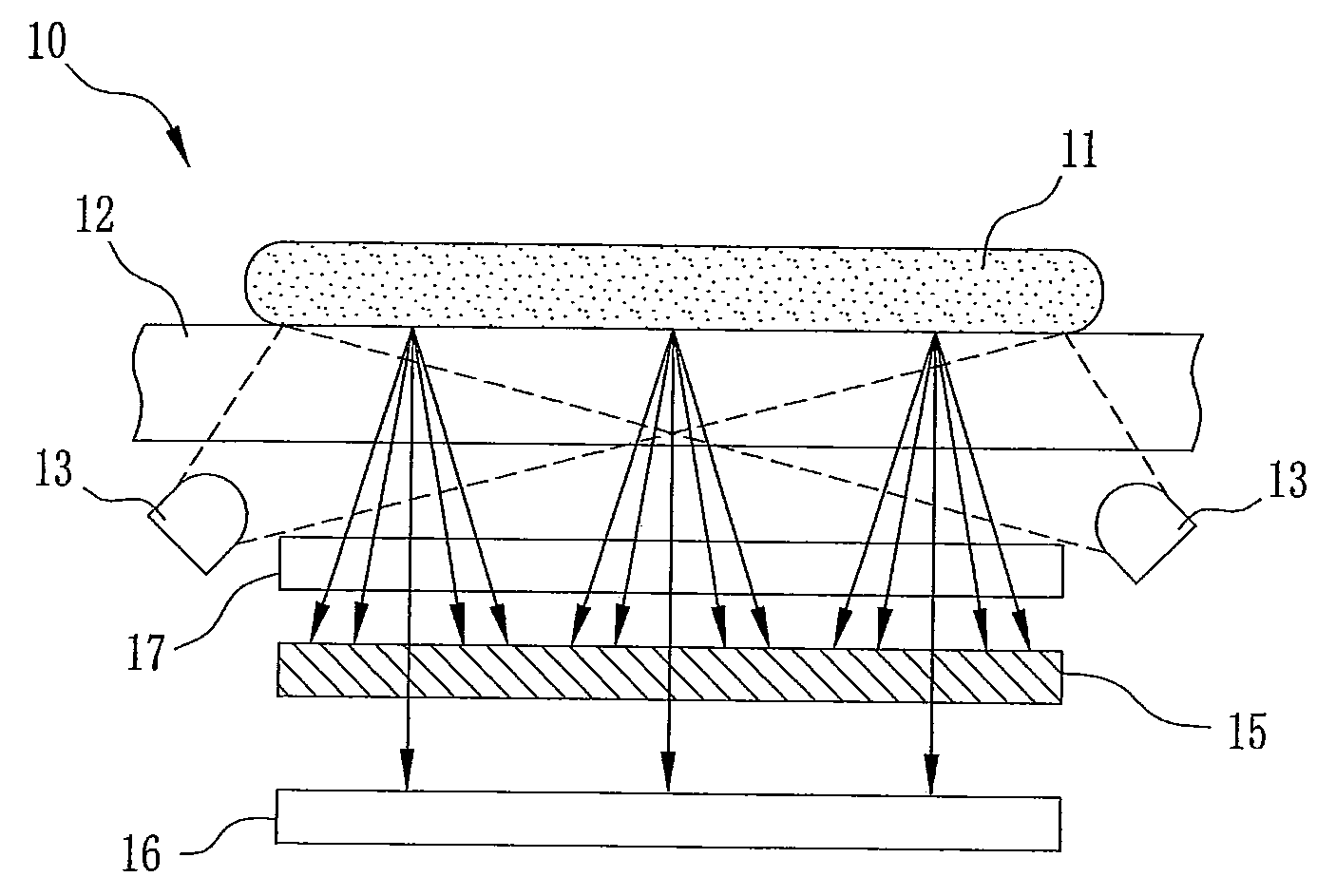
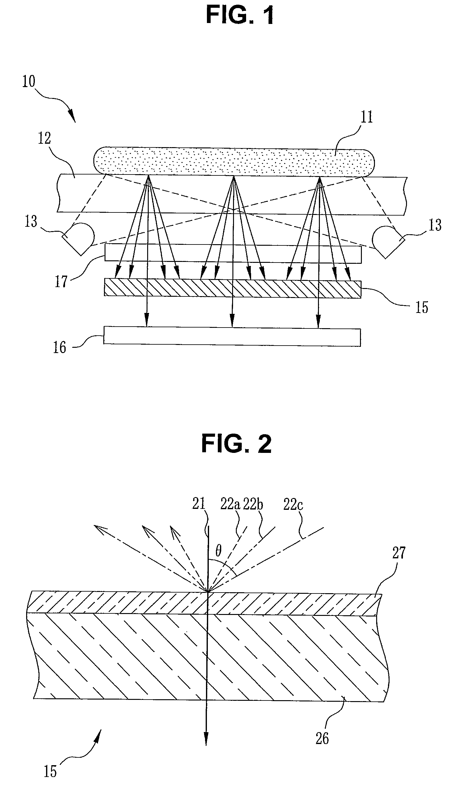
[0036]As shown in FIG. 1, a close contact type imaging device 10 is an imaging device for acquiring an image of an object 11 close to the image sensor 16 and, in particular, an imaging device suitable for acquiring an image of an object 11 almost in close contact to the image sensor 16. The close contact type imaging device 10 has a protection cover 12, an LED 13, an angle limiting filter 15 (optical filter), and an image sensor 16. The protection cover 12 is composed of a transparent glass plate and protects from scratches or dust the angle limiting filter 15 and the image sensor 16 arranged below. Further, the object 11 whose image is to be acquired is placed directly on the protection cover 12.

[0037]The LED 13 emits infrared light having a wavelength of 850 nm, and illuminates the object 11 uniformly from a location under the protection cover 12. The infrared light emitted from the LED 13 is scattered in accordance with the absorption coefficient and the reflectivity for infrared...

example 1

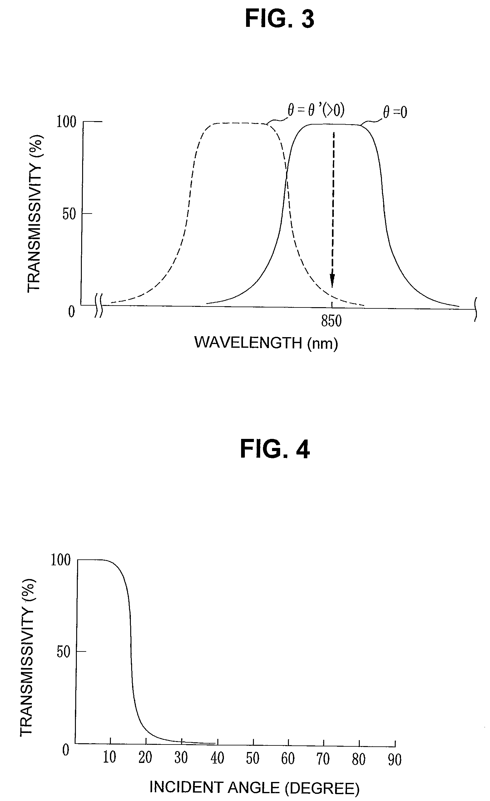
[0050]As shown in Table 1, the angle limiting filter 15 of low directivity was fabricated such that a dielectric multilayer film 27 composed of tantalum pentoxide (Ta2O5) having a refractive index of 2.1136 and silicon oxide (SiO2) having a refractive index of 1.4525 was provided on a glass substrate 26 having a refractive index of 1.51. The dielectric multilayer film 27 of the angle limiting filter 15 of low directivity was composed of a stack of 66 layers fabricated by alternately stacking tantalum pentoxide films and silicon oxide films each having an optical film thickness 0.25 to 1.0 at a reference wavelength of 850 nm.

TABLE 1MaterialntAir1.00001Ta2O52.11360.252SiO21.45250.023Ta2O52.11360.254SiO21.45250.505Ta2O52.11360.256SiO21.45250.257Ta2O52.11360.758SiO21.45250.259Ta2O52.11360.2510SiO21.45250.2511Ta2O52.11360.7512SiO21.45250.2513Ta2O52.11360.2514SiO21.45250.2515Ta2O52.11360.5016SiO21.45250.2517Ta2O52.11360.2518SiO21.45250.2519Ta2O52.11360.2520SiO21.45250.2521Ta2O52.11360.252...

example 2

[0055]As shown in Table 2, the angle limiting filter 15 of high directivity was fabricated such that a dielectric multilayer film 27 composed of tantalum pentoxide having a refractive index of 2.1136 and silicon oxide having a refractive index of 1.4525 was provided on a glass substrate 26 having a refractive index of 1.51. The dielectric multilayer film 27 of the angle limiting filter 15 of high directivity was composed of a stack of 90 layers or the like fabricated by almost alternately stacking tantalum pentoxide films and silicon oxide films each having an optical film thickness 0.25 to 1.5 at a reference wavelength of 850 nm.

TABLE 2MaterialntAir1.00001SiO21.45250.3035122Ta2O52.11360.0943753Ta2O52.11360.254SiO21.45250.255Ta2O52.11360.256SiO21.45250.257Ta2O52.14360.258SiO21.45250.259Ta2O52.11360.2510SiO21.45250.2511Ta2O52.11360.2512SiO21.45250.2513Ta2O52.11360.2514SiO21.45250.2515Ta2O52.11360.2516SiO21.45250.2517Ta2O52.11361.5018SiO21.45250.2519Ta2O52.11360.2520SiO21.45250.2521Ta...


PUM


Abstract

A close contact type imaging device is an imaging device for acquiring an image of an object in a state that the object is in close contact to an image sensor. This imaging device has an angle limiting filter. The angle limiting filter is constructed from: a glass substrate of a parallel plate; and a dielectric multilayer film provided on the glass substrate. This angle limiting filter transmits light within a particular wavelength range approximately perpendicularly incident onto the surface, and shields light outside the particular wavelength range and light within the particular wavelength obliquely incident onto the surface.

Description

[0001]This application is based on and claims priority under 35 U.S.C §119 from Japanese Patent Application No. 2008-139109, filed on May 28, 2008, the entire disclosure of which is herein incorporated by reference.BACKGROUND OF THE INVENTION[0002]1. Field of the Invention[0003]The present invention relates to an imaging device for acquiring an image of an object located at a predetermined position by utilizing light within a particular wavelength range and, in particular, to an imaging device of close contact type for acquiring an image of an object in a state that the object is almost in close contact to an image sensor.[0004]2. Description of Related Art[0005]Imaging devices are widely used that acquire images of manuscripts such as printed images, documents, and bar code images. As examples of such imaging devices, imaging devices of close contact type are known in which image acquisition is performed in a state that a line image sensor having the same width as a manuscript to b...

Claims


Application Information

Patent Timeline
IPC IPC(8): H01L27/00G01J3/50
CPCG03B11/04G03B11/00G03B15/03
Inventor KURAHASHI, HAJIMEMATSUSHITA, HIDEYUKI
Owner FUJIFILM CORP
Why Eureka
Try Eureka