LED lighting module

a technology of led lighting and diodes, which is applied in the direction of lighting and heating apparatus, semiconductor devices for light sources, instruments, etc., can solve the problems of difficult to precisely match the design, the profile of the lens is not easy to shape, and the lens is more difficult to form on such a device, so as to reduce the occurrence of flares, effectively outputting indirect light, and economic and effective

Inactive Publication Date: 2009-12-03
ADVANCED OPTOELECTRONICS TECH
View PDF13 Cites 98 Cited by
  • Summary
  • Abstract
  • Description
  • Claims
  • Application Information

AI Technical Summary

Benefits of technology

[0009]One aspect of the present invention provides an economical and effective LED lighting module capable of laterally emitting light. Such an LED lighting module is applicable to illumination apparatuses for effectively outputting indirect light. The original lighting area of an LED, a point light source, is increased through the operation of the LED lighting module. Accordingly, the occurrence of flares is reduced. Such an LED lighting module can be applied to advertising display apparatuses, and a uniform surface light source is easily obtained for improving display quality. The LED lighting module of the present invention is also applicable to the backlight module of an LCD.

Problems solved by technology

As shown in FIG. 1A, the profile of the lens is not easy to shape, and cannot be accurately formed to precisely match its design.
Furthermore, the LED is a small scale device, and hence, such complicated lens is more difficult to form on such a device.
The requirement of such complicated lenses demands sophisticated processes and high manufacturing costs.
Therefore, such LEDs are not suitable for mass production.

Method used


Image

  • LED lighting module
  • LED lighting module
  • LED lighting module

Examples


Embodiment Construction

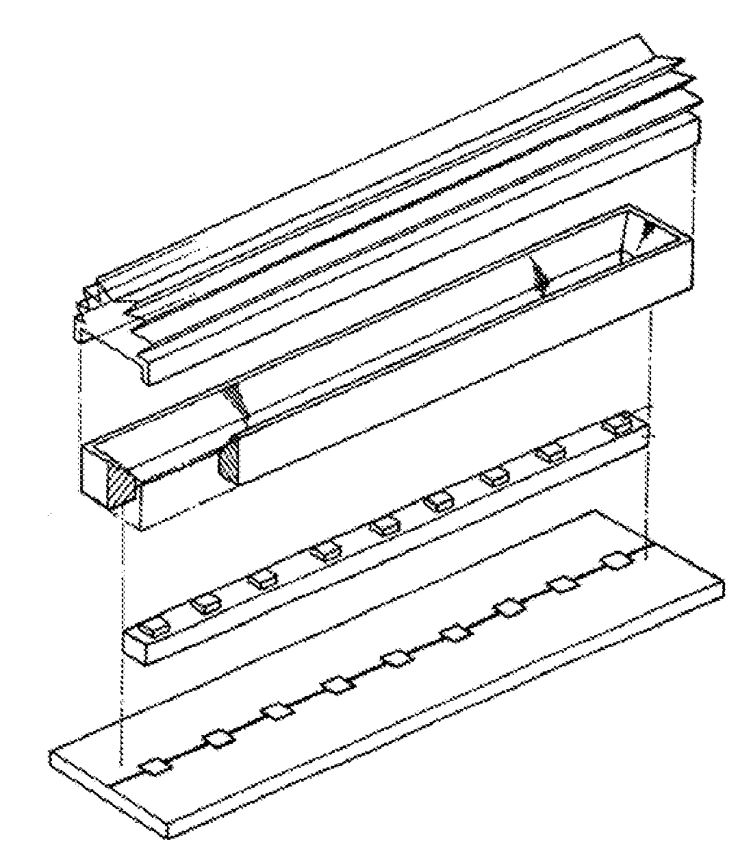
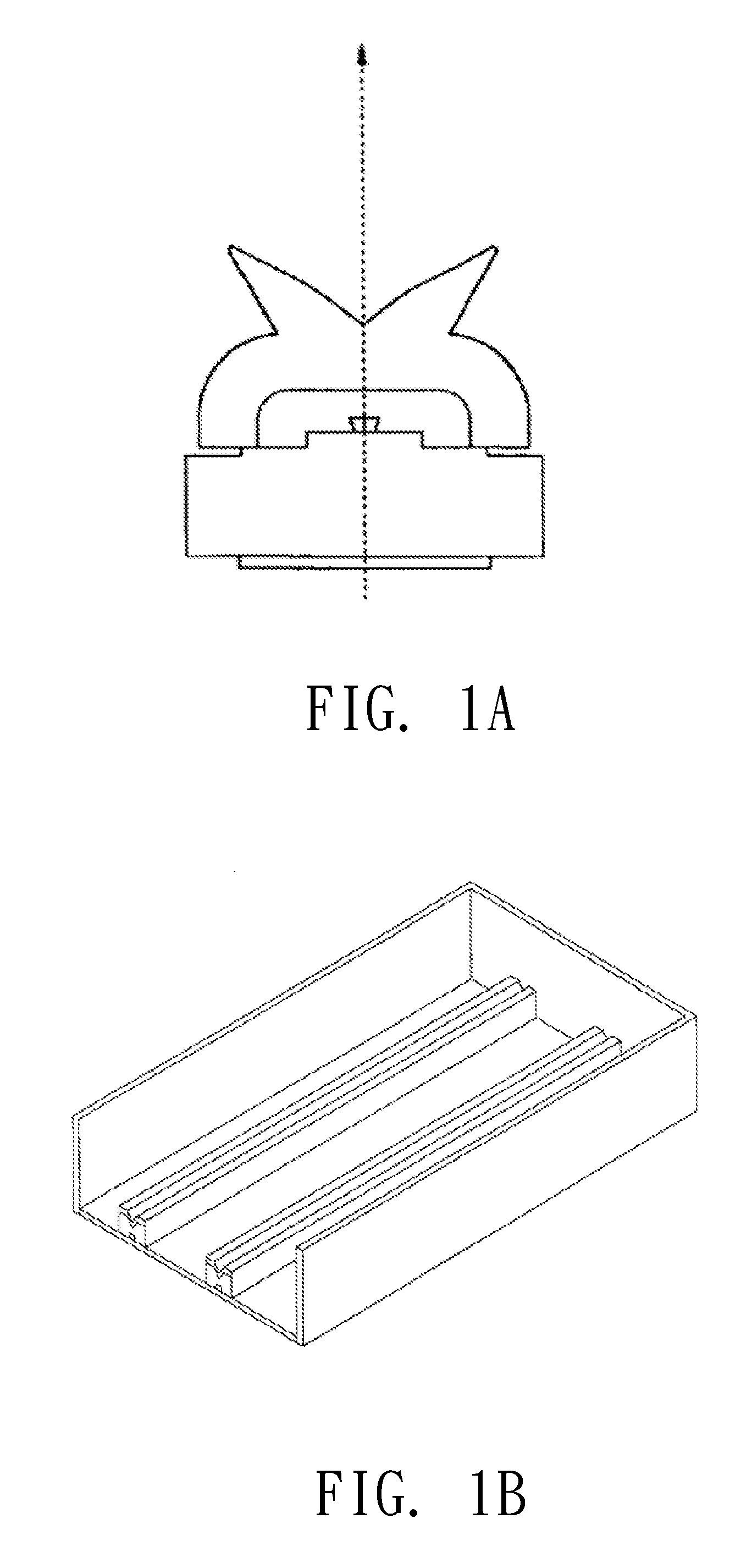
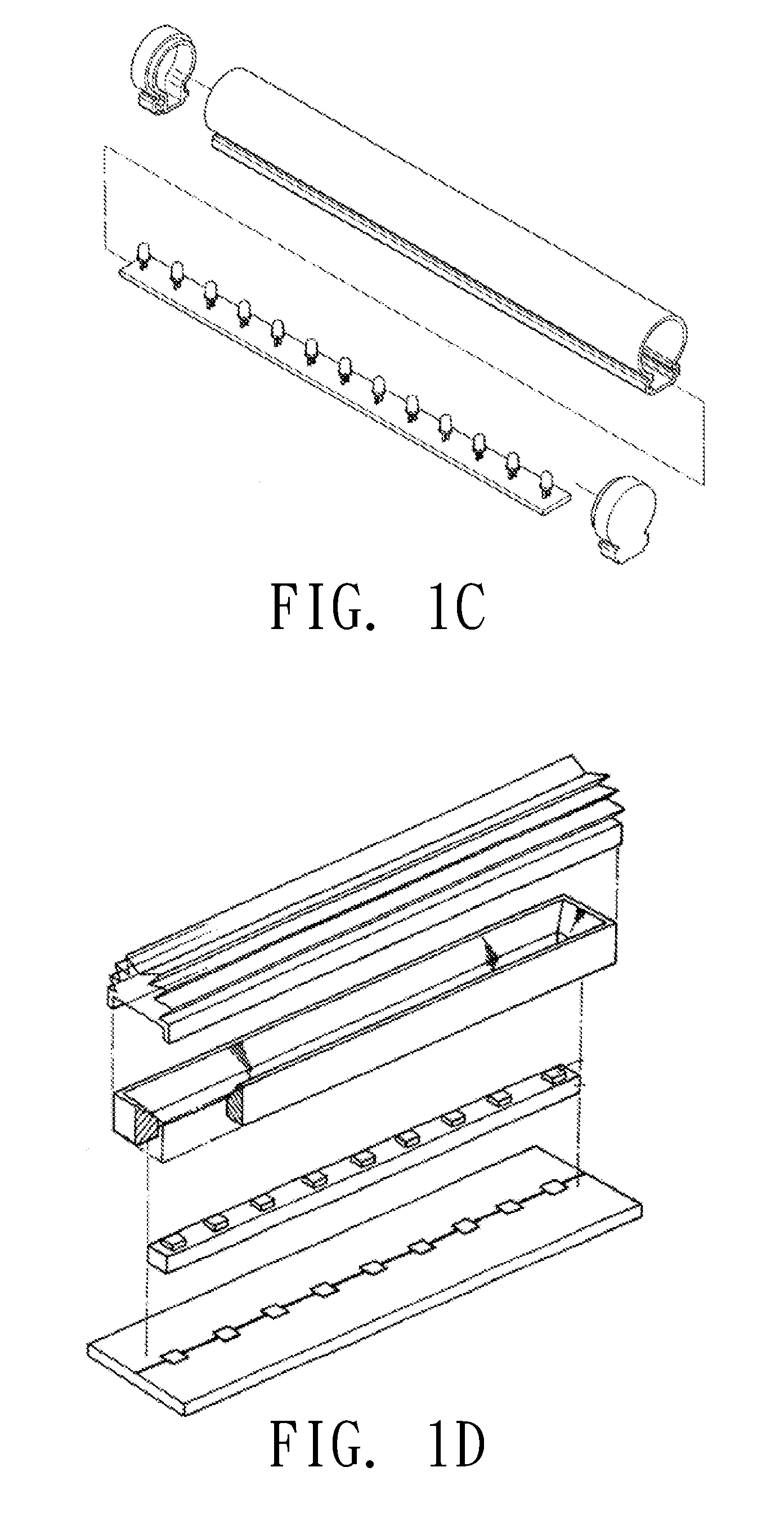
[0033]The present invention provides an LED (light emitting diode) lighting module. For complete understanding of the present invention, the following description will present in detail the manufacturing steps and the composition. The present invention is not limited by the specified particulars of a backlight module that are familiar to persons skilled in the art. In addition, well-known compositions or steps are not described in detail so as to avoid any additional limitation. The preferable embodiments of the present invention are described in detail. In addition to the detailed descriptions, the present invention also can be applied to other embodiments. Therefore, the scope of the present invention is not limited, and is dependent on the following claims.

[0034]Taiwan Patent No. 1244227 discloses a lighting source of a backlight module employing LEDs. The lighting source employs LEDs with a COB (chip on board) package type. That is, LED dies are directly mounted on substrates. T...


PUM


Abstract

An LED lighting module comprises an array luminous element and a bar-like light guiding structure. The array luminous element comprises a plurality of illuminants of top-emitting LEDs arranged in an array form. The bar-like light guiding structure surrounds two laterals of the array luminous element. The bar-like light guiding structure comprises a first curved surface and a second curved surface. The first curved surface and the second curved surface respectively descend toward the middle of the array luminous element from the two sides of the array luminous element, and meet above the middle of the array luminous element. The first curved surface and the second curved surface connect with each other at the plane with a certain angle and in tangency where the positive optical axis exists. The positive optical axis is the direction perpendicular to the plane on which the LEDs are mounted.

Description

BACKGROUND OF THE INVENTION[0001](A) Field of the Invention[0002]The present invention relates to an LED (light emitting diode) lighting module, and more particularly, to an LED lighting module which is bar-like and side-emitting.[0003](B) Description of the Related Art[0004]The light emitting diode (LED) offers several advantages over previous light sources including low energy consumption, high efficiency, long lifetime and low environmental pollution (e.g., mercury-free construction), and is generally applied to the back light modules of various flat displays for excellent color expression. Therefore, the use of LEDs in flat-screen display applications is of high importance, and the related technology is developing rapidly.[0005]Back light modules are classified according to the position of the light source, the main classifications being a side type and a direct type. Currently, LCDs (liquid crystal display) are mainly applied to notebook computers and LCD monitors whose back li...

Claims


Application Information

Patent Timeline
Patent Type & Authority Applications(United States)
IPC IPC(8): F21S4/00
CPCF21S4/003F21V5/04F21V7/0091F21Y2103/003G02B6/0018F21Y2105/001G02F1/133603G02F1/133605G02F1/133611G02F2001/133607F21Y2101/02G02B6/0021F21S4/20F21Y2103/10F21Y2105/10F21Y2115/10G02F1/133607
Inventor WU, WEI HUNGCHANG, CHIA CHEN
Owner ADVANCED OPTOELECTRONICS TECH
Why Eureka
Try Eureka