Mugfet with stub source and drain regions

a finfet and source technology, applied in the field of microelectronics, can solve the problems of reducing the density of devices for a given area of the substrate, and and achieve the effect of reducing the density of devices

Inactive Publication Date: 2009-12-10
GLOBALFOUNDRIES INC
View PDF35 Cites 26 Cited by
  • Summary
  • Abstract
  • Description
  • Claims
  • Application Information

AI Technical Summary

Benefits of technology

[0005]In one embodiment, the present invention provides a method of forming a finFET that does not include the traditional angled implants for providing the source / drain / extension / halo regions of the device. Traditionally, the formation of the source and drain regions of a prior finFET includes angled implants in order to ensure uniform doping along the fin sidewall at the gate / spacer edge. Unfortunately, when block masks are used to selectively dope the devices, i.e., finFET devices, of a first type conductivity, such as nFET, but not the devices of a second type conductivity, such as pFETs, the physical separation between the different types of devices that is required to avoid shadowing during implantation typically results in a density penalty, i.e., decreased density of devices for a given area of the substrate.

Problems solved by technology

Unfortunately, when block masks are used to selectively dope the devices, i.e., finFET devices, of a first type conductivity, such as nFET, but not the devices of a second type conductivity, such as pFETs, the physical separation between the different types of devices that is required to avoid shadowing during implantation typically results in a density penalty, i.e., decreased density of devices for a given area of the substrate.

Method used


Image

  • Mugfet with stub source and drain regions
  • Mugfet with stub source and drain regions
  • Mugfet with stub source and drain regions

Examples


Embodiment Construction

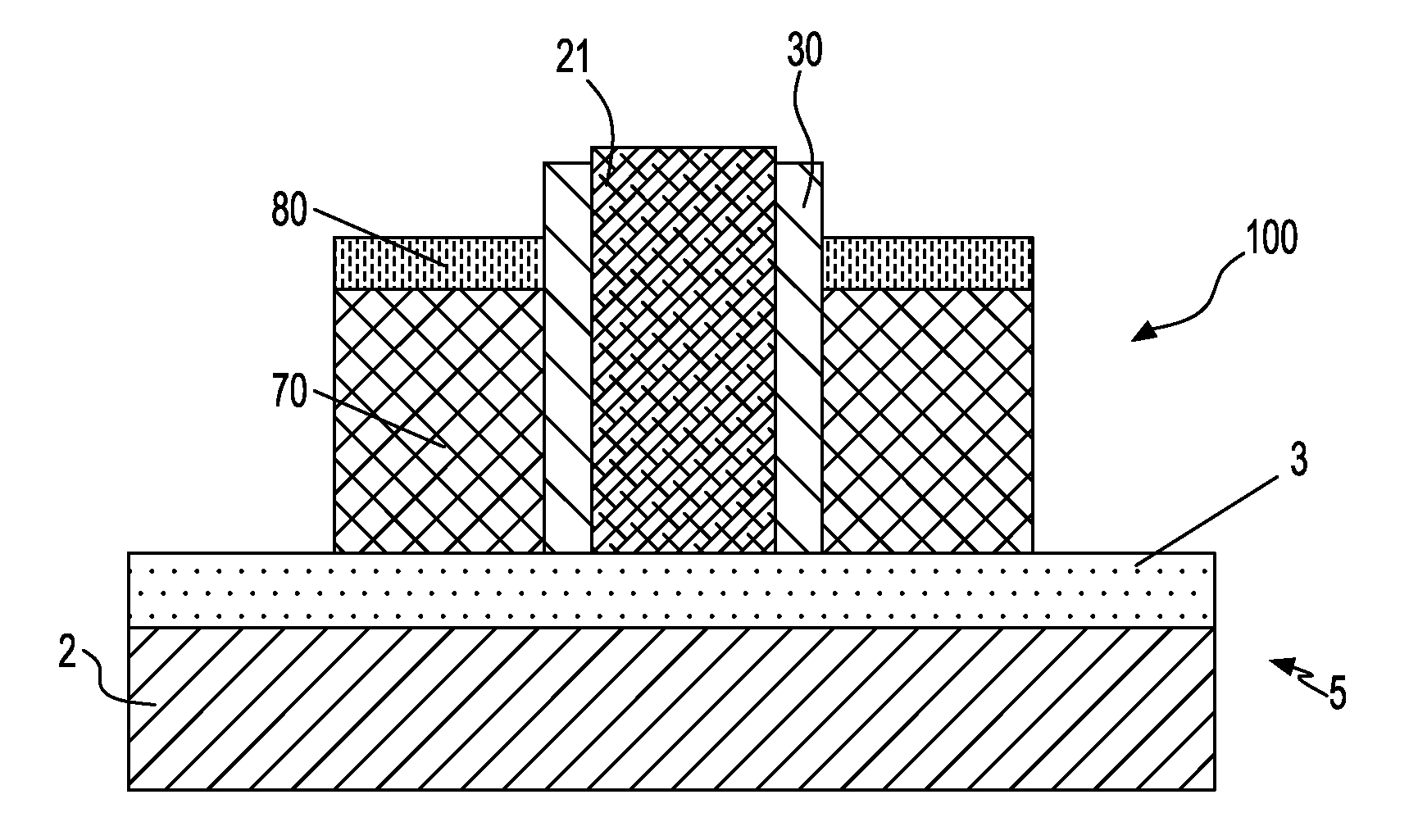
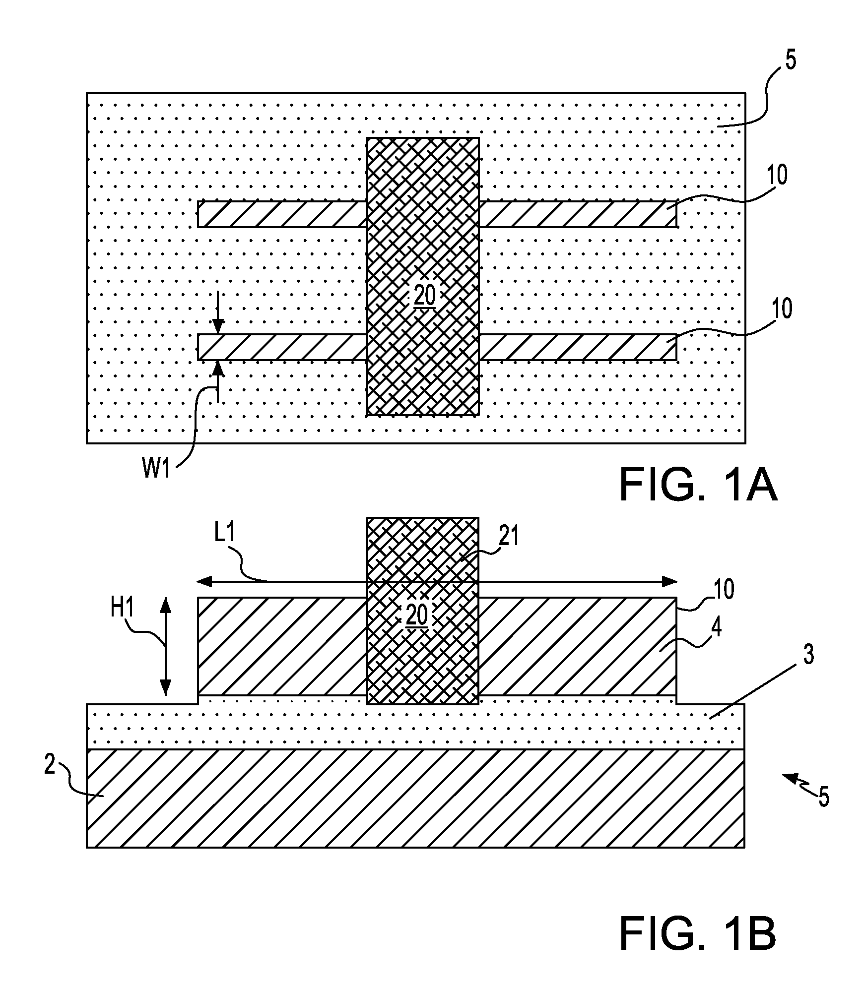
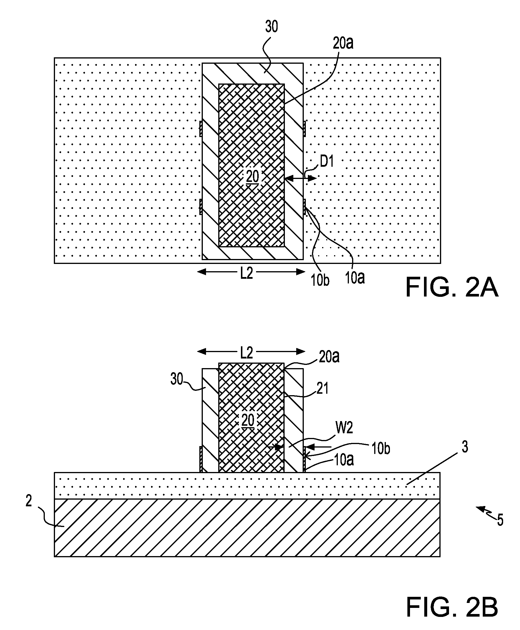
[0030]Detailed embodiments of the present invention are disclosed herein; however, it is to be understood that the disclosed embodiments are merely illustrative of the invention that may be embodied in various forms. In addition, each of the examples given in connection with the various embodiments of the invention are intended to be illustrative, and not restrictive. Further, the figures are not necessarily to scale, some features may be exaggerated to show details of particular components. Therefore, specific structural and functional details disclosed herein are not to be interpreted as limiting, but merely as a representative basis for teaching one skilled in the art to variously employ the present invention.

[0031]The present invention relates to structures and methods for forming a semiconductor device. In one embodiment, the present invention relates to structures and methods for forming finFET semiconductor devices. When describing the following structures and methods, the fo...


PUM


Abstract

The present invention provides a semiconductor device that includes at least one semiconductor Fin structure atop the surface of a substrate; the semiconducting fin structure including a channel of a first conductivity type and source/drain regions of a second conductivity type, the source/drain regions present at each end of the semiconductor fin structure; a gate structure immediately adjacent to the semiconductor fin structure, a dielectric spacer abutting each sidewall of the gate structure wherein the each end of the fin structure extends a dimension that is less than about ¼ a length of the Si-containing fin structure from a sidewall of the dielectric spacer; and a semiconductor region to the each end of the semiconductor fin structure, wherein the semiconductor region to the each end of the semiconductor fin structure is separated from the gate structure by the dielectric spacer.

Description

FIELD OF THE INVENTION[0001]The present invention relates to microelectronics. In one embodiment, the present invention provides a method of forming a finFET device.BACKGROUND OF THE INVENTION[0002]The dimensions of semiconductor field effect transistors (FETs) have been steadily shrinking over the last thirty 30 years or so, as scaling to smaller dimensions leads to continuing device performance improvements. Planar FET devices have a conducting gate electrode positioned above a semiconducting channel, and electrically isolated from the channel by a thin layer of gate oxide. Current through the channel is controlled by applying voltage to the conducting gate.[0003]For a given device length, the amount of current drive for an FET is defined by the device width. Current drive scales proportionally to device width, with wider devices carrying more current than narrower devices. Different parts of integrated circuits (ICs) require the FETs to drive different amounts of current, i.e., w...

Claims


Application Information

Patent Timeline
Patent Type & Authority Applications(United States)
IPC IPC(8): H01L29/00H01L21/8236
CPCH01L29/785H01L29/66803
Inventor ANDERSON, BRENT A.BRYANT, ANDRESNOWAK, EDWARD J.
Owner GLOBALFOUNDRIES INC
Why Eureka
Try Eureka