Solid-state imaging apparatus

a solid-state imaging and apparatus technology, applied in the field of solid-state imaging apparatus, can solve the problems of increasing the width between pixels, serious layout limitations of a/d converters b, etc., and achieve the effect of reducing the pitch of pixels

Inactive Publication Date: 2009-12-10
CANON KK
View PDF15 Cites 53 Cited by
  • Summary
  • Abstract
  • Description
  • Claims
  • Application Information

AI Technical Summary

Benefits of technology

[0009]An object of the present invention is to provide a solid-state imaging apparatus which can easily reduce pixel arrangement pitch in a direction along a row.

Problems solved by technology

Meanwhile, with miniaturization of pixels, serious limitations in layout are posed to the A / D converters 9 arranged at the respective columns.
The configuration disclosed in FIG. 8 has the problem of increase in the width between the pixels because a plurality of accumulation units is arranged in the direction along the row.

Method used


Image

  • Solid-state imaging apparatus
  • Solid-state imaging apparatus
  • Solid-state imaging apparatus

Examples


first embodiment

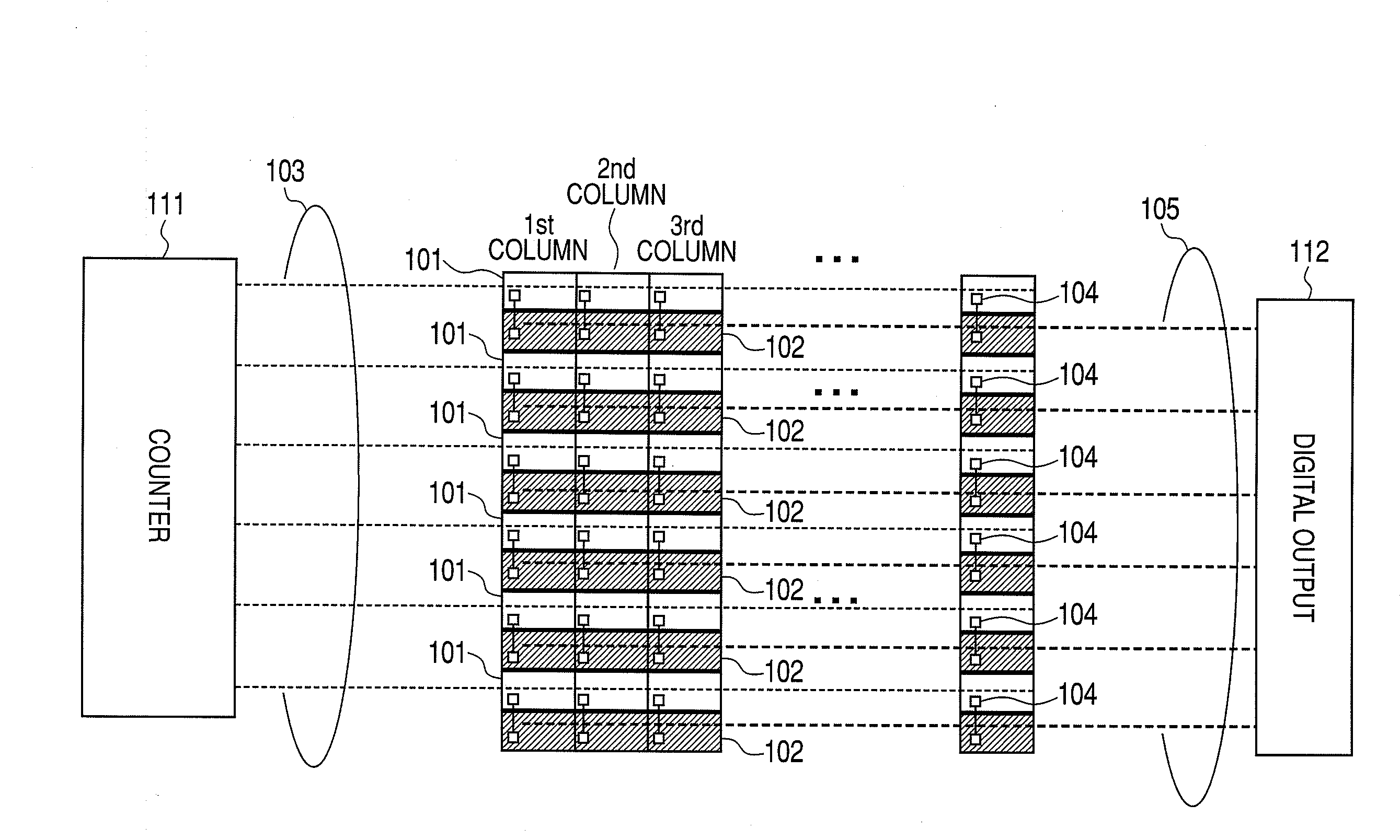
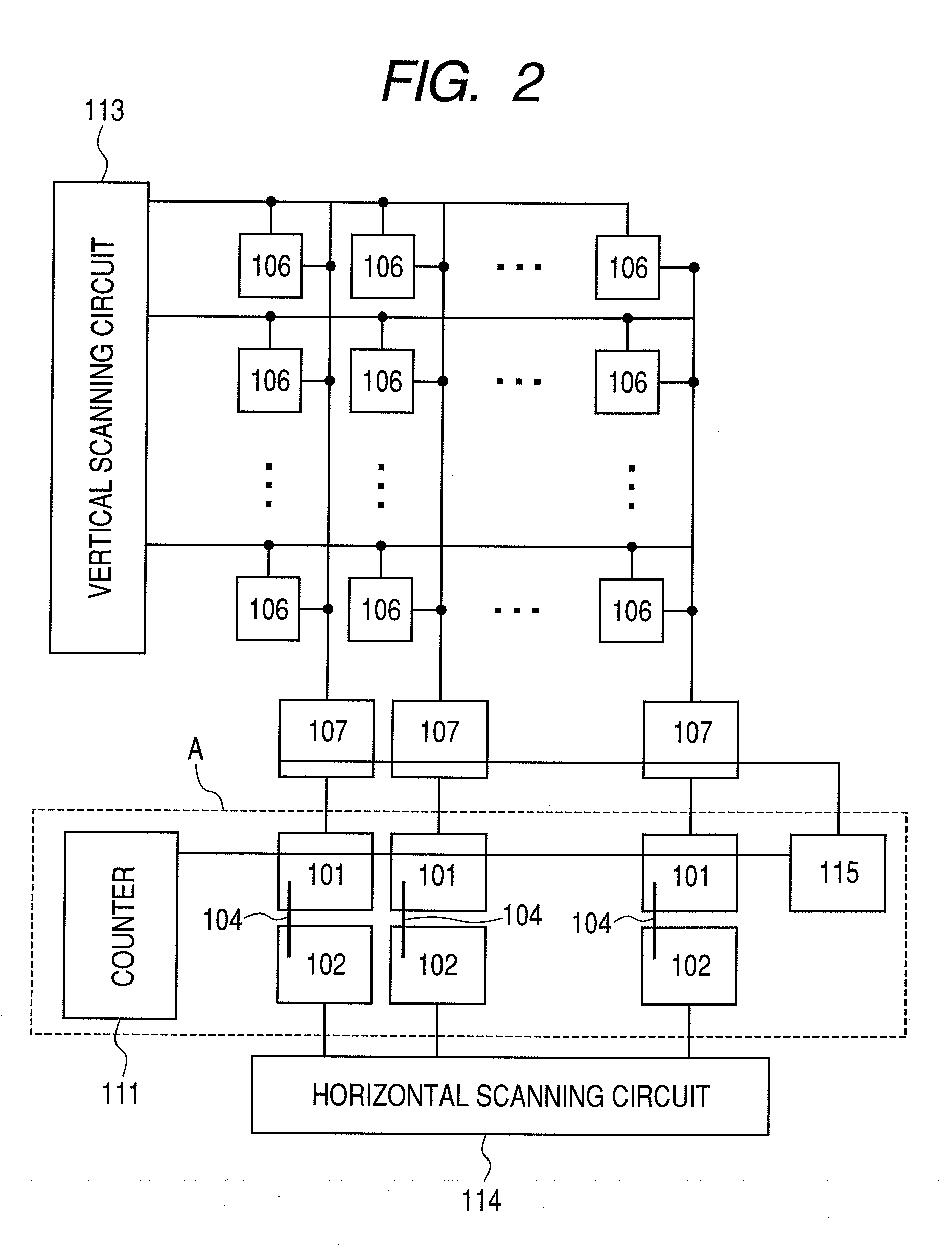
[0022]FIG. 2 is a diagram illustrating a configuration example of a solid-state imaging apparatus according to a first embodiment of the present invention. Pixels 106 are arranged in a two-dimensional array. The pixel 106 includes a photodiode, for example, and generates an image signal based on photoelectric conversion. Each of the pixels includes an amplifying unit which outputs a voltage signal based on an electric charge generated in the photodiode. A vertical scanning circuit 113 selects the pixels 106 by row unit, and reads out analog signals generating in the selected pixels 106 in A / D (analog / digital) converters 107 in a direction along a column. The A / D converter 107 is arranged at each of the columns of the pixels 106, and converts an analog signal into a digital signal. A counter 111 is arranged commonly to respective columns of the pixels 106 to count a digital signal value. First accumulation units 101, of which number is n, are arranged corresponding to each column of ...

second embodiment

[0031]FIG. 3 is a diagram showing another configuration example of the region A of FIG. 2 according to a second embodiment of the present invention. The same components as in FIGS. 1 and 2 are shown by the same reference numerals and characters. Accumulation unit groups each made by the first accumulation unit 101 and the second accumulation unit 102 arranged adjacently in a direction along the row and paired, of which number is n, are arranged in the direction along the column.

[0032]The inter-accumulation unit wiring 104 is connected between the first accumulation unit 101 and the second accumulation unit 102 adjacent in the direction along the row. The data line 103 is connected to the first accumulation unit 101. The output line 105 is connected to the second accumulation unit 102. In the present embodiment, the pixel arrangement pitch in the direction along the row also can be easily reduced by arranging each of the accumulation unit groups arranged correspondingly to each pixel...

third embodiment

[0034]FIG. 4 is a diagram illustrating another configuration example of the region A of FIG. 2 according to a third embodiment of the present invention. The same components as those in FIGS. 1 and 2 are shown by the same reference numerals and characters.

[0035]An accumulation unit group 1 is provided, in which the first accumulation unit 101 and the second accumulation unit 102 are adjacently arranged in the direction along the column in the arrangement order of the first accumulation unit 101—the second accumulation unit 102 and are paired. An accumulation unit group 2 is provided, in which the first accumulation unit 101 and the second accumulation unit 102 are adjacently arranged in the direction along the column in the arrangement order of the second accumulation unit 102—the first accumulation unit 101. The accumulation unit group 1 and the accumulation unit group 2 are adjacently arranged repeatedly in the arrangement order of the accumulation unit group 1—the accumulation uni...


PUM


Abstract

A solid-state imaging apparatus comprises first accumulation units, of which number is n, holding a digital value of n-bits output from a counter, second accumulation units, of which number is n, holding the digital value of n-bits transferred from the first accumulation units, of which number is n, and an A/D converter writing the digital value of n-bits from the counter based on an image signal generated by pixels into the first accumulation units, of which number is n, wherein correspondingly to each column of the pixels, the first accumulation unit of m-th bit (1≦m≦n) and the second accumulation unit of m-th bit (1≦m≦n) are arranged and paired, and the pairs of which number is n are arranged in a direction along the column of pixels.

Description

BACKGROUND OF THE INVENTION[0001]1. Field of the Invention[0002]The present invention relates to a solid-state imaging apparatus.[0003]2. Description of the Related Art[0004]In recent years, the number of pixels of a solid-state imaging apparatus has been increased for enhancement of the quality of photographed images, in an image input apparatus such as a digital still camera and a digital video camera. Further, the solid-state imaging apparatuses, which are loaded with A / D converters to realize digital output, come out.[0005]As one example of the A / D conversion type which is loaded on a solid-state imaging apparatus, there is a column A / D conversion type. As the prior art document, Japanese Patent Application Laid-Open No. H05-48460 (Patent Document 1) is cited. Its circuit configuration is illustrated in the drawing.[0006]A column A / D conversion type has A / D converters 9 at respective columns of pixels and operates them in parallel, and therefore, can enhance the speed of readout...

Claims


Application Information

Patent Timeline
Patent Type & Authority Applications(United States)
IPC IPC(8): H04N5/335H03M1/12H03M1/56H04N1/40H04N5/369H04N5/374H04N5/378
CPCH04N5/37455H04N25/772
Inventor SHIBATA, MASANORIKOBAYASHI, MASAHIROKIKUCHI, SHINHIYAMA, HIROKI
Owner CANON KK
Why Eureka
Try Eureka