Method for designing light transmission device, optical element and sensor

a technology of light transmission device and optical element, applied in the direction of optical radiation measurement, instruments, polarising elements, etc., can solve the problems of aperture array, unavoidable broadening of transmission spectrum, and unavoidable decrease of transmittan

Inactive Publication Date: 2009-12-17
CANON KK
View PDF6 Cites 20 Cited by
  • Summary
  • Abstract
  • Description
  • Claims
  • Application Information

AI Technical Summary

Problems solved by technology

However, there has been a problem that when the aperture size is enlarged, the width of the transmission spectrum unavoidably becomes broad because light quantity transmitting without being affected by plasmon increases, and when the aperture size is reduced, a transmittance unavoidably decreases.
On the other hand, the aperture array has characteristics like a filter, but has not always had high S / N (signal-to-noise ratio).

Method used


Image

  • Method for designing light transmission device, optical element and sensor
  • Method for designing light transmission device, optical element and sensor
  • Method for designing light transmission device, optical element and sensor

Examples


embodiment i-1

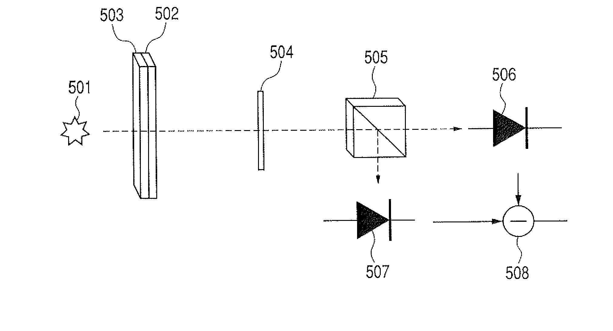
[0085]FIG. 5 illustrates a color filter for use in color separation, which is an example of a light transmission device obtained by using the present invention.

[0086]When light is incident on a rectangular aperture array 503 which is a set of rectangular apertures 502 formed in a metal thin film 501, localized plasmon is excited in an interface of a metal. Then, the light passes through the aperture in a form of plasmon, is united with propagation light on the back face, and transmits.

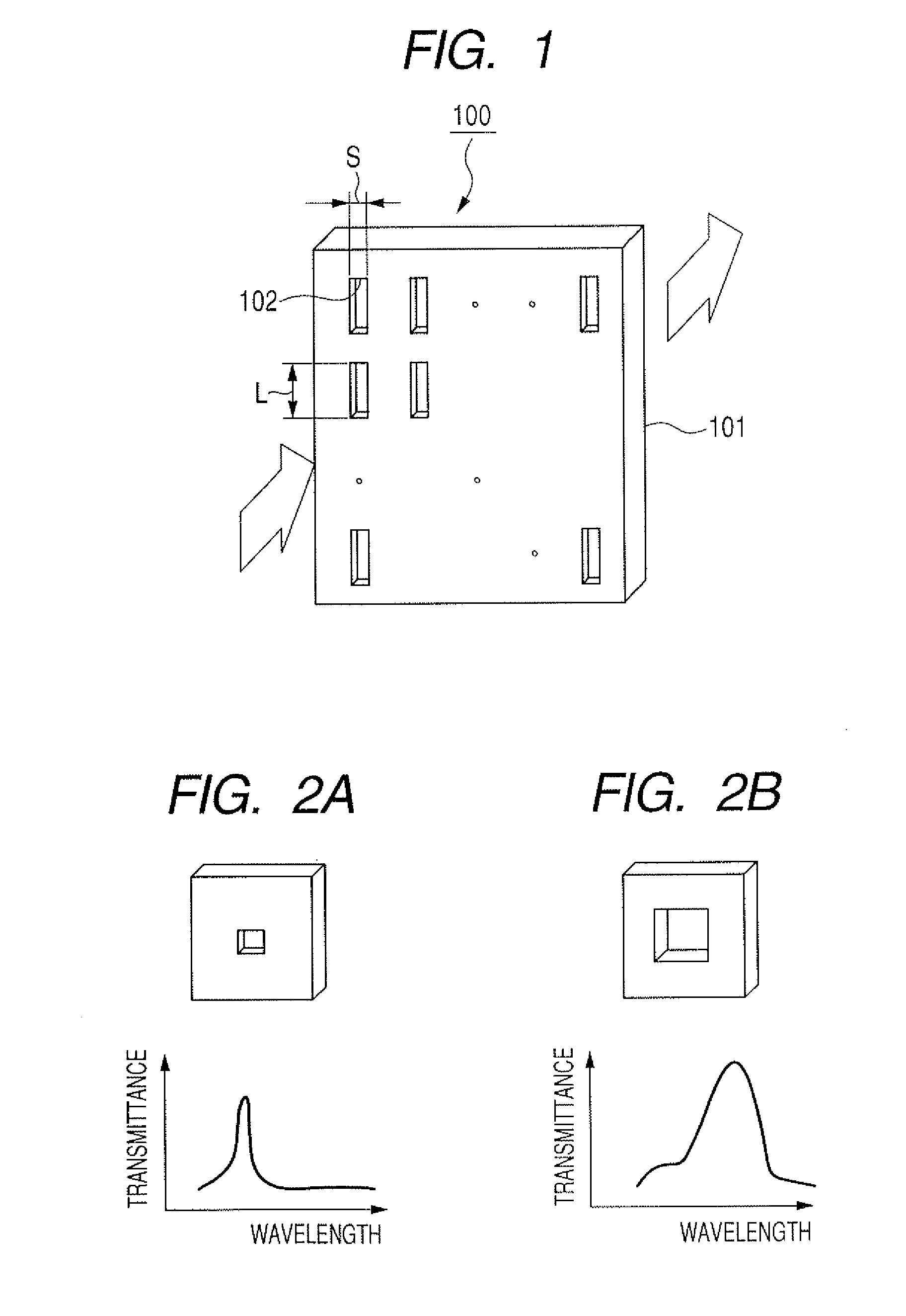
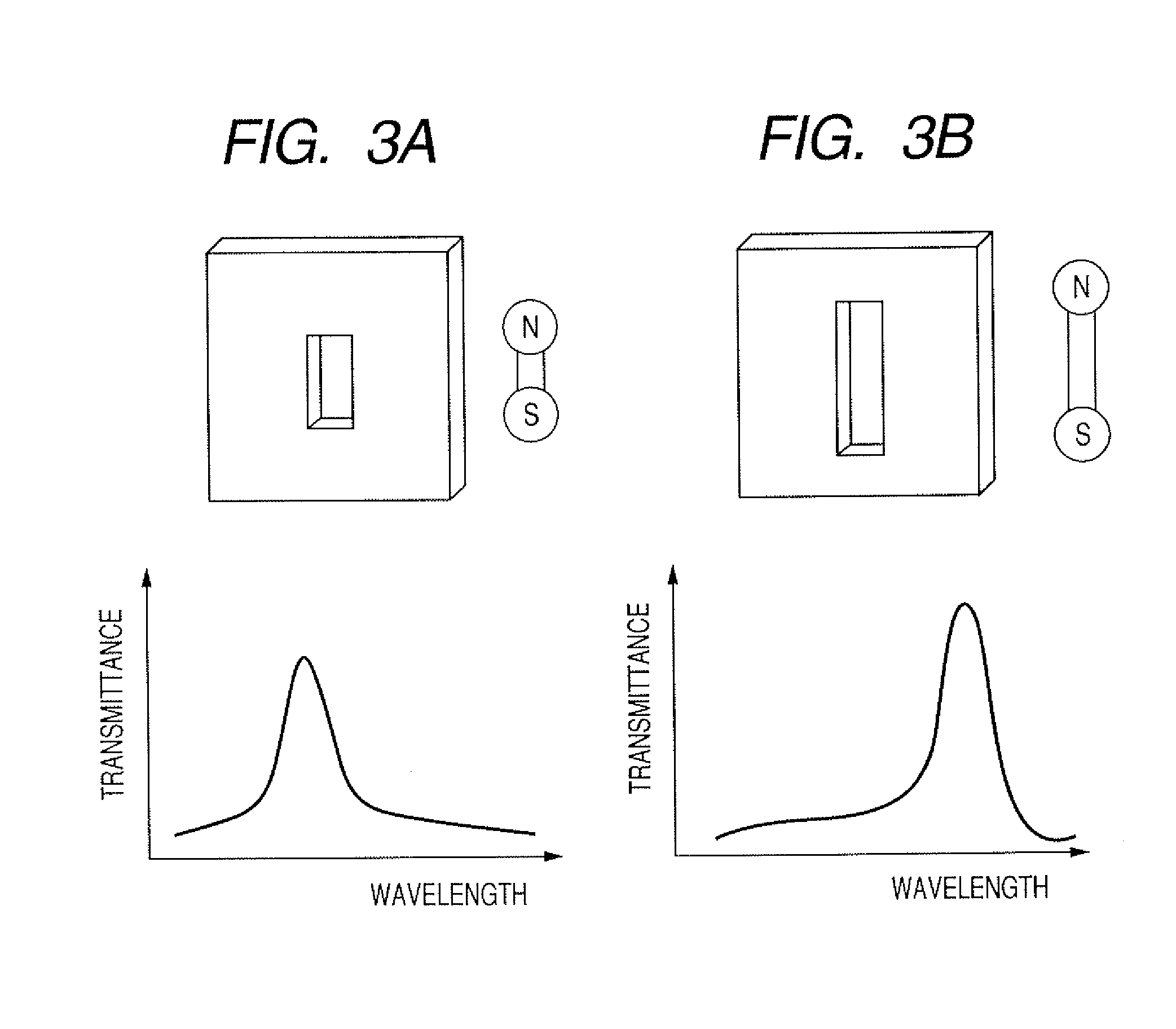
[0087]Transmitted light has a peak wavelength depending on a shape of a rectangular aperture 502, because of being affected by localized plasmon resonance. Rectangular apertures 502 are arranged in a two-dimensional array form, but may also be arranged in a one-dimensional array form. The rectangular aperture 502 includes a plurality of types of the rectangular apertures 502R, 502G and 502B, of which the dimension of long side are different from the others. A rectangular aperture array 503 includes rec...

embodiment i-2

[0093]FIG. 7 illustrates a conceptual diagram of an optical switching element which is an example of a light transmission device obtained by using the present invention.

[0094]The optical switching element polarizes white light emitted from a light source 706 by using a polarizer 702, and makes the polarized light pass through a rectangular aperture array 703. The optical switching element can change the chromaticness of transmitted light by polarizing the while light by using the polarizer 702.

[0095]In the present embodiment, a short side dimension of a rectangular aperture is determined so as not to be excessively small in comparison with a wavelength of irradiation light, and so as to give a necessary intensity of transmitted light even to a polarized light in a minor axis direction.

[0096]A rectangular aperture (not shown) in a rectangular aperture array 703 has characteristics of making polarized light pass therethrough in different manners depending on a polarization direction o...

embodiment i-3

[0102]FIG. 10 illustrates a conceptual diagram of an example of a chemical sensor device by using the present invention.

[0103]The chemical sensor device makes a light source 1006 arranged on an incident plane side of a rectangular aperture array 1003 which is a light transmission device, project light toward the rectangular aperture array 1003, and makes a device 1004 for detecting a spectrum of the transmitted light, which is placed on the exit plane side of the rectangular aperture array 1003, receive the transmitted light.

[0104]An object 1005 to be measured is placed on a rectangular aperture array 1003 so as to closely contact with each other. The chemical sensor device makes a device 1004 for detecting the spectrum obtain a transmission spectrum, and detect a change in a peak wavelength or peak intensity of transmitted light to chemically sense a substance to be inspected.

[0105]The chemical sensor device can sense the substance 1005 to be inspected at high sensitivity, by makin...


PUM


Abstract

The present invention provides a method for designing a light transmission device, which adjusts a wavelength region of a spectrum of transmitted light without expanding a width of a transmission spectrum and without lowering the transmittance. The method for designing a light transmission device having a metal thin film, and a rectangular aperture which is formed in a plane of the metal thin film, has a long side and a short side and makes light pass therethrough, wherein the short side has a dimension smaller than a wavelength of incident light, and the long side is determined to have such a dimension that a peak wavelength at which the transmittance of light passing through the rectangular aperture is maximal can be a predetermined value.

Description

TECHNICAL FIELD[0001]The present invention relates to a method for designing a light transmission device, an optical element and a sensor.BACKGROUND ART[0002]Conventionally, a method of making use of the absorption of a coloring matter or a method of making use of the Bragg reflection of a dielectric multilayer has been used in a device for filtering an electromagnetic wave.[0003]On the other hand, it has been revealed in recent years that light abnormally passes through a circular aperture formed in a metal thin film caused by localized plasmon resonance, so that the wavelength can be selected and light can be condensed, as is disclosed in Japanese Patent No. 3,008,931.[0004]When light passes through a circular or square aperture formed in a metal thin film, the transmission spectrum changes depending on an aperture size (or side length).[0005]However, there has been a problem that when the aperture size is enlarged, the width of the transmission spectrum unavoidably becomes broad ...

Claims


Application Information

Patent Timeline
Patent Type & Authority Applications(United States)
IPC IPC(8): G01J3/04G02B5/00G02B5/20G02B5/30
CPCG02B5/204G02B5/008
Inventor OGINO, MASAYAYAMADA, TOMOHIRONISHIUMA, SATORUMIZUTANI, NATSUHIKOKURODA, RYO
Owner CANON KK
Why Eureka
Try Eureka