Dye-sensitized solar cell and process for producing the same

a solar cell and dye sensitization technology, applied in the field of dye sensitization solar cell and a process for producing the same, can solve the problems of increasing the thickness of the porous semiconductor layer, complex and costly, and the process is not suitably applicable in the case of porous semiconductor layer thickness exceeding 13 m, and achieves high conversion efficiency

Inactive Publication Date: 2009-12-24
NIPPON STEEL CHEMICAL CO LTD +1
View PDF4 Cites 28 Cited by
  • Summary
  • Abstract
  • Description
  • Claims
  • Application Information

AI Technical Summary

Benefits of technology

[0021]In the dye-sensitized solar cell of the present invention, a conductive metal film having a large number of randomly located penetrations is formed in the interior of or on the conductive-substrate-side surface of its porous semiconductor layer, whereby it can be produced easily; and moreover, even in the case where the thickness of the porous semiconductor layer is increased, a high conversion efficiency can be obtained.
[0022]The process for producing a dye-sensitized solar cell of the present invention includes: a first step in which the porous semiconductor layer is formed on the transparent conductive film; a second step in which a fine-particle layer made up of fine particles removable by heating or solvent-cleaning is formed on the surface of the porous semiconductor layer; a third step in which a conductive metal film is formed on the surface of the fine-particle layer; and a fourth step in which the fine-particle layer is made to disappear by heating or solvent-cleaning. Alternatively, the process includes: a first step in which the porous semiconductor layer is formed on the transparent conductive film; a second step in which a mixed layer of a porous semiconductor material and fine particles removable by heating or solvent-cleaning is formed on the surface of the porous semiconductor layer; a third step in which a conductive metal film is formed on the surface of the mixed layer; and a fourth step in which the fine particles are made to disappear by heating or solvent-cleaning, or the process includes: a step of forming the porous semiconductor layer on the surface of the transparent conductive film; a step of forming, on the surface of the porous semiconductor layer, a mixed layer of a conductive metal and fine particles removable by heating or solvent-cleaning; and a step of making the fine particles disappear by heating or solvent-cleaning, and further includes a fifth step in which a porous semiconductor layer, different from the porous semiconductor layer formed in the first step, is formed on the surface of the conductive metal film, whereby the conductive metal film having a large number of randomly located penetrations can be formed reliably in an easy manner.

Problems solved by technology

However, increasing the thickness of the porous semiconductor layer also presents some problems.
Further, the process disclosed in Japanese Patent Laid-Open No. 2003-197283, in which a comb-shaped conductive layer is formed in the metal oxide semiconductor layer by vacuum deposition, has the effect of improving the conversion efficient, but will be complicated and costly.
Moreover, whether or not the process is suitably applicable to cases where the thickness of the porous semiconductor layer exceeds 13 μm has not yet been proven.
Besides, there is a limit to decreasing the thickness of the wire-mesh-like structure, and thus, the process may present the problem of short-circuit due to the contact of the wire-mesh-like structure with the counter electrode.

Method used


Image

  • Dye-sensitized solar cell and process for producing the same
  • Dye-sensitized solar cell and process for producing the same
  • Dye-sensitized solar cell and process for producing the same

Examples


examples

[0064]The present invention will be further described by Examples and Comparative examples. It is to be understood that Examples below are not intended to limit the present invention.

examples 1 to 4

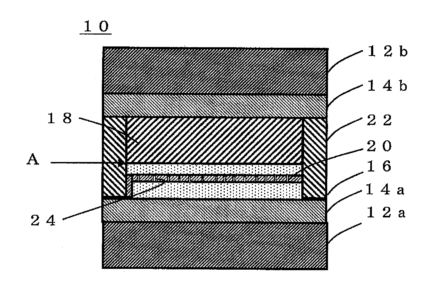
[0065]Borosilicate glass with a transparent conductive film 20 mm×30 mm in dimensions and 1 mm in thickness was coated with titanium oxide nanoparticle paste (particle size: 20 nm) and burned at 500° C. to prepare a titanium oxide porous film (porous semiconductor layer) with thickness 15 μm.

[0066]On the titanium oxide porous film was formed a tungsten (W) film (conductive metal film) having a thickness t in the range of 50 to 150 nm and penetrations with an average pore size of about 3 μm. On the tungsten (W) film was formed a titanium oxide porous film, one as described above, with thickness 15 μm. Then, the film was immersed into an aqueous solution of titanium tetrachloride and heated at 500° C. N3 dye (manufactured by Solaronix) was used.

[0067]This film, together with an FTO film having a platinum film formed on its surface by sputtering, as a counter electrode, was sealed with a 50-μm spacer. An electrolyte prepared by dissolving 250 ml of I2 and 580 mM of t-BuPy in acetonitri...

examples 4 , 5

Examples 4, 5

[0070]Borosilicate glass with a transparent conductive film 20 mm×10 mm in dimensions and 1 mm in thickness was coated with titanium oxide nanoparticle paste (particle size: 20 nm) and burned at 500° C. to prepare a titanium oxide porous film with thickness 30 μm.

[0071]On the titanium oxide porous film was formed a tungsten film having a thickness t in the range of 40 to 120 nm and penetrations with an average pore size of about 3 μm. Then, the film was immersed into an aqueous solution of titanium tetrachloride and heated at 500° C. N719 dye was used.

[0072]This film, together with an FTO film having a platinum film formed on its surface by sputtering, as a counter electrode, was sealed with a 50-μm spacer. An electrolyte prepared by dissolving 250 ml of I2 and 580 mM of t-BuPy in acetonitrile was injected into the resultant cell in order to produce a cell. The obtained cell was evaluated in the same manner as in Examples 1 to 3.


PUM

PropertyMeasurementUnit
thicknessaaaaaaaaaa
thicknessaaaaaaaaaa
thickaaaaaaaaaa

Abstract

A dye-sensitized solar cell is provided, wherein it can be produced by a relatively easy and simple process and ensures high conversion efficiency even in cases where the thickness of the porous semiconductor layer is increased. The dye-sensitized solar cell 10 includes, in the interior of or on the conductive-substrate-side surface of the porous semiconductor layer 16, conductive metal film 20, such as a film of tungsten, having a large number of randomly located penetrations 24. Penetrations 24 of the conductive metal film 20 are formed by forming a fine-particle layer on the surface of the porous semiconductor layer, forming a conductive metal film on the surface of the fine-particle layer, and making the fine-particle layer disappear by heating or solvent-cleaning.

Description

TECHNICAL FIELD[0001]The present invention relates to a dye-sensitized solar cell and a process for producing the same.BACKGROUND ART[0002]Dye-sensitized solar cells are known as wet solar cells or Grätzel cells, which are characterized by being produced without silicon semiconductor and having an electrochemical cell structure using an electrolysis solution represented by an iodine solution. Specifically, dye-sensitized solar cells have a simple structure which includes: a porous semiconductor layer, such as titania layer formed by baking titanium dioxide powder on a transparent conductive glass plate (a transparent substrate having a transparent conductive film laminated on its surface) and making the powder adsorb a dye; a counter electrode made up of a conductive glass plate (a conductive substrate); and an electrolysis solution, such as an iodine solution, arranged between the porous semiconductor layer and the counter electrode.[0003]Dye-sensitized solar cells have attracted c...

Claims


Application Information

Patent Timeline
Patent Type & Authority Applications(United States)
IPC IPC(8): H01L31/00H01L31/18
CPCH01G9/2022Y02E10/542H01G9/2059H01G9/2031Y02P70/50
Inventor HAYASE, SHUZISHIRATSUCHI, RYUICHIOHKUBO, SUEHIROYAMAGUCHI, YOSHIHIRO
Owner NIPPON STEEL CHEMICAL CO LTD
Why Eureka
Try Eureka