This helps you quickly interpret patents by identifying the three key elements:
Problems solved by technology
Method used
Benefits of technology
Benefits of technology
[0011]According to another aspect of the invention, there is provided A light emitting device including: a light emitting element made of nitridesemiconductor; a first lead including a die pad portion at its one end portion, the light emitting element being bonded to the die pad portion; a second lead with its one end portion being opposed to the one end portion of the first lead; a resin molded body including a recess with at least part of the die pad portion being exposed to the bottom thereof so that emission light from the light emitting element can be emitted upward, a lower surface with at least part of the lower surface of the first lead and at least part of the lower surface of the second lead being exposed thereto, and a lateral surface with at least part of the lateral surface of the die pad portion being exposed thereto, the resin molded body embedding the first lead and the second lead so that the other end portion of the first lead and the other end portion of the second lead are projected in directions opposite to each other; and a sealing resin mixed with phosphor that can absorb the emission light and emit wavelength-converted light having a longer wavelength than the emission light, the sealing resin being filled in the recess so as to cover the light emitting element, the at least part of the lateral surface of the die pad portion which is exposed being located on a first plane which is generally coplanar with the lateral surface of the other end portion of the first lead and the lateral surface of the other end portion of the second lead, and mixed light of the emission light and the wavelength-converted light being able to be emitted.
Problems solved by technology
However, even in this technique, heat dissipation is not sufficient and puts limitations on high-current operation.
Furthermore, the process for manufacturing the lead frame is complicated by the bending work and insufficient in volume productivity.
Method used
Image
Click on the blue label to locate the original text in one second.
Reading with bidirectional positioning of images and text.
Examples
first embodiment
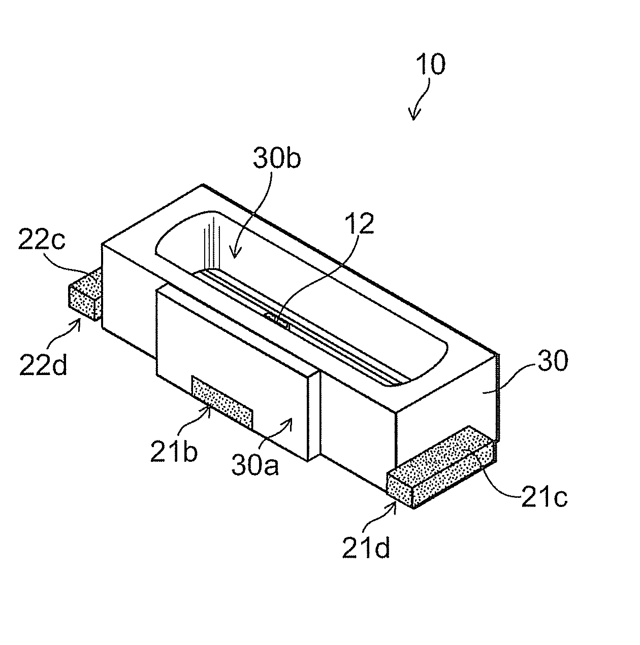
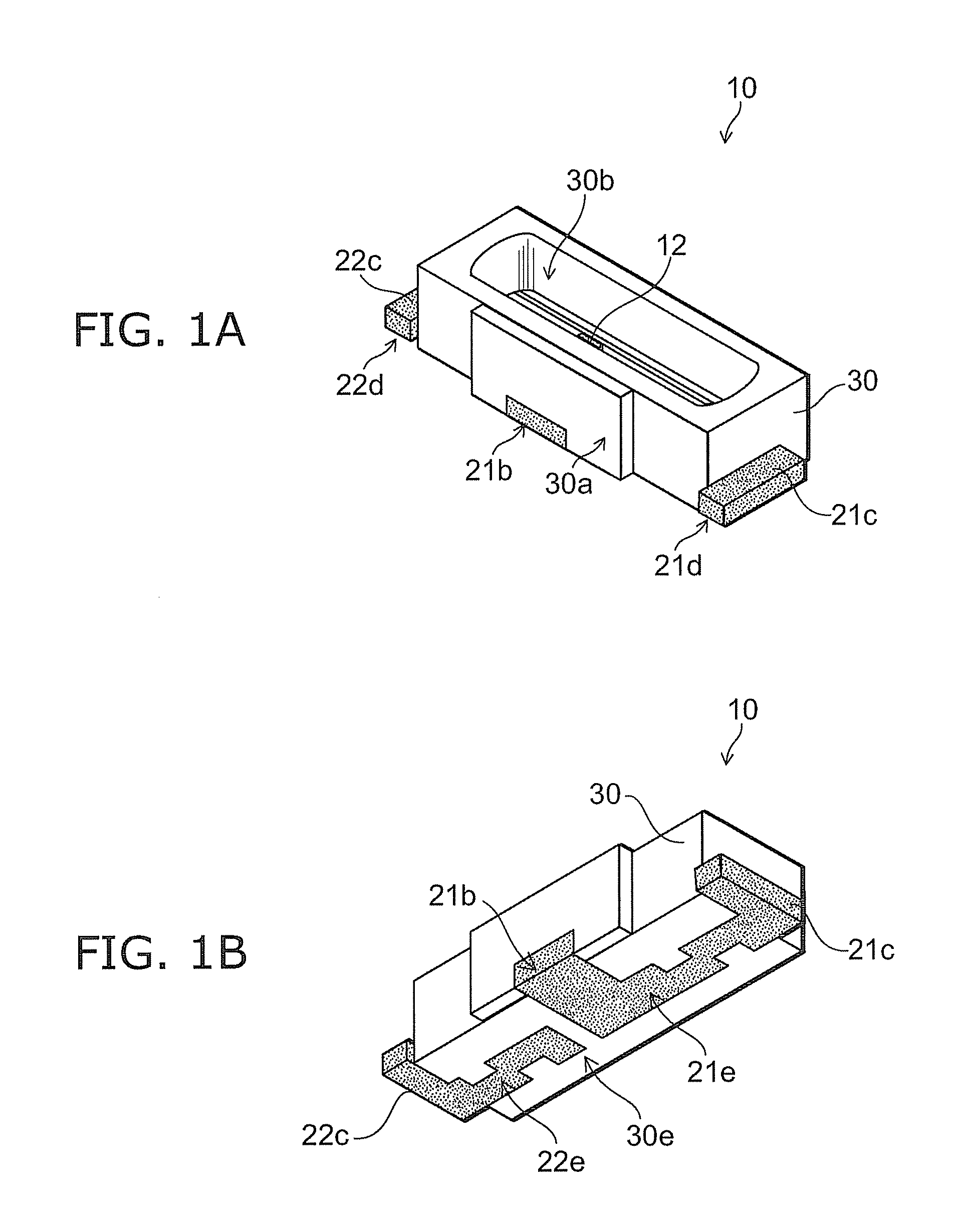
[0020]FIG. 1 is a schematic view of a light emitting device according to the invention. More specifically, FIG. 1A is a perspective view from obliquely above, and FIG. 1B is a perspective view from obliquely below. It is noted that FIG. 1 shows the situation before the resin sealing process.
[0021]A first lead 21 and a second lead 22 are embedded in a (resin) molded body 30 illustratively made of a thermoplastic or thermoset resin. The first lead 21 has an end portion 21c projected from the molded body 30, and the second lead 22 has an end portion 22c projected from the molded body 30. The end portions 21c and 22c are generally collinear and projected in opposite directions.
[0022]The molded body 30 has a recess 30b. Each upper surface of the first lead 21 and the second lead 22 is exposed to the bottom of the recess 30b. A light emitting element 12 made of semiconductor is bonded to the exposed surface of the first lead 21 in the recess 30b.
[0023]On the lateral surface side of the m...
second embodiment
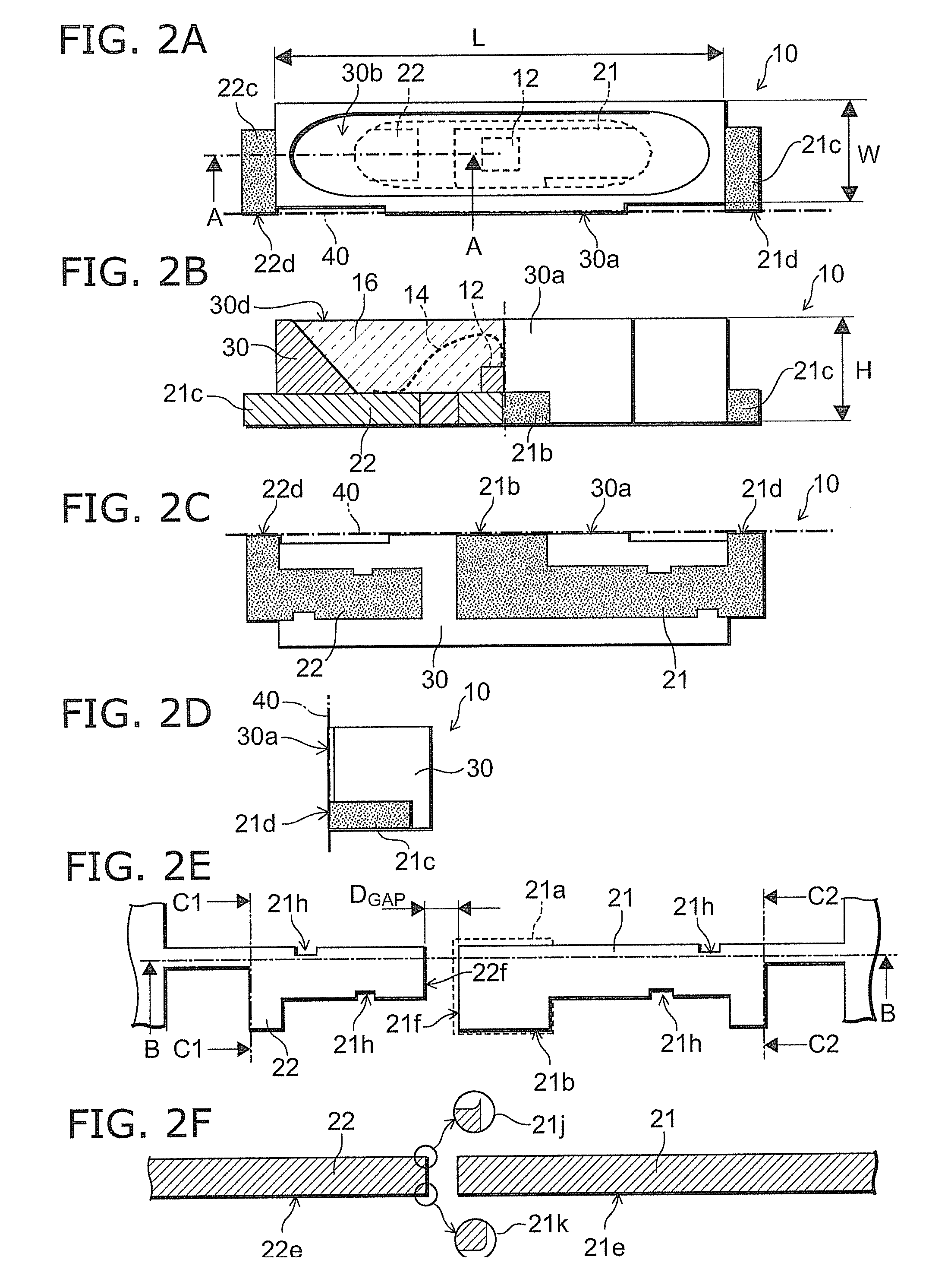
[0052]FIG. 5 is a schematic view of a light emitting device according to a More specifically, FIG. 5A is a plan view, and FIG. 5B is a partial cross-sectional view taken along line A-A.
[0053]The lateral surface 30a of the molded body 30 has a notch 30c in the neighborhood of the lateral surface 21b of the first lead 21. Part of the die pad portion 21a is projected from this notch 30c. Such a projection allows the device to be soldered so that the solder wraps around the upper surface, the lateral surface, and the lower surface of the die pad portion 21a, whether the device is used as a top-emitting device or a laterally emitting device. Thus, bonding strength can be increased.
[0054]It is noted that as shown in FIG. 5A, the lateral surface 30a located on the first plane 40 is present on both outer sides of the notch 30c as viewed from above. Hence, in the case where the device is attached as a laterally emitting device, the device is supported at five points with respect to the surf...
third embodiment
[0055]FIG. 6 is a schematic view of a light emitting device according to a More specifically, FIG. 6A is a plan view, FIG. 6B is a partial cross-sectional view taken along line A-A, FIG. 6C is a side view, FIG. 6D is a plan view of the lead frame, and FIG. 6E is a cross-sectional view of the lead frame taken along line B-B.
[0056]In this embodiment, a recess 21m is formed in the first lead 21 illustratively by press working, and a light emitting element 12 is bonded to the bottom surface of the recess 21m. The sidewall of the recess 21m serves as a reflecting surface of the emission light to enhance upward light. To provide the recess 21m, the first lead 21 is designed to have a large thickness, e.g., 0.25 to 0.4 mm. This facilitates reducing thermal resistance.
[0057]The resin molded body 30 and the sealing resin 16 filled in its recess 30b may be discolored by absorbing UV to visible light. Hence, in the neighborhood of the light emitting element 12 where the light intensity is hig...
PUM
Abstract
A light emitting device includes: a light emitting element; a first lead including a die pad portion at its one end portion, the light emitting element being bonded to the die pad portion; a second lead with its one end portion being opposed to the one end portion of the first lead; and a resin molded body including a recess with at least part of the die pad portion being exposed to the bottom thereof so that emission light from the light emitting element can be emitted upward, a lower surface with at least part of the lower surface of the first lead and at least part of the lower surface of the second lead being exposed thereto, and a lateral surface with at least part of the lateral surface of the die pad portion being exposed thereto, the resin molded body embedding the first lead and the second lead so that the other end portion of the first lead and the other end portion of the second lead are projected in directions opposite to each other. The at least part of the lateral surface of the die pad portion which is exposed is located on a first plane which is generally coplanar with the lateral surface of the other end portion of the first lead and the lateral surface of the other end portion of the second lead.
Description
CROSS-REFERENCE TO RELATED APPLICATIONS[0001]This application is based upon and claims the benefit of priority from the prior Japanese Patent Application No. 2008-159120, filed on Jun. 18, 2008; the entire contents of which are incorporated herein by reference.BACKGROUND OF THE INVENTION[0002]1. Field of the Invention[0003]This invention relates to a light emitting device.[0004]2. Background Art[0005]Semiconductor light emitting devices capable of emitting light in the visible wavelength range are used for backlight sources and indicators of car-mounted and other illumination devices and image display devices. In these applications, surface-mounted devices facilitate high-density packaging on a substrate or other mounting member.[0006]For example, in application to the backlight source of an image display device, the display plate is placed on the light guide plate so that the display screen faces upward. To apply light to the lateral side of the light guide plate along the surface ...
Claims
Application Information
Patent Timeline
Application Date:The date an application was filed.
Publication Date:The date a patent or application was officially published.
First Publication Date:The earliest publication date of a patent with the same application number.
Issue Date:Publication date of the patent grant document.
PCT Entry Date:The Entry date of PCT National Phase.
Estimated Expiry Date:The statutory expiry date of a patent right according to the Patent Law, and it is the longest term of protection that the patent right can achieve without the termination of the patent right due to other reasons(Term extension factor has been taken into account ).
Invalid Date:Actual expiry date is based on effective date or publication date of legal transaction data of invalid patent.

