CMOS devices having reduced threshold voltage variations and methods of manufacture thereof

Inactive Publication Date: 2009-12-24
GLOBALFOUNDRIES INC
View PDF9 Cites 11 Cited by
  • Summary
  • Abstract
  • Description
  • Claims
  • Application Information

AI Technical Summary

Benefits of technology

[0007]The shortcomings of the prior art are overcome and additional advantages are provided through the provision of methods for fabricating NFET and PFET devices that share a common gate electrode with an air gap between the N-type and P-type doped regions of the gate electrode for inhibiting dopant cross-diffusion. In one embodiment, a method of forming an integrated circuit comprising an NFET transistor and a PFET transistor that share a common gate electrode comprises: depositing and patterning a first gate electrode section

Problems solved by technology

Demands for increased performance, functionality, and manufacturing economy for integrated circuits have resulted in extreme integration density and scaling of NFETs and PFETs to very small sizes.
Unfortunately, reducing the spacing between NFET and PFET devices sharing a common gate electrode can lead to dopant cross-diffusion between the NFET and PFET sections of the gate electrode.
This cross-diffusion

Method used


Image

  • CMOS devices having reduced threshold voltage variations and methods of manufacture thereof
  • CMOS devices having reduced threshold voltage variations and methods of manufacture thereof
  • CMOS devices having reduced threshold voltage variations and methods of manufacture thereof

Examples


Example

[0013]The detailed description explains the preferred embodiments of the invention, together with advantages and features, by way of example with reference to the drawings.

DETAILED DESCRIPTION OF THE INVENTION

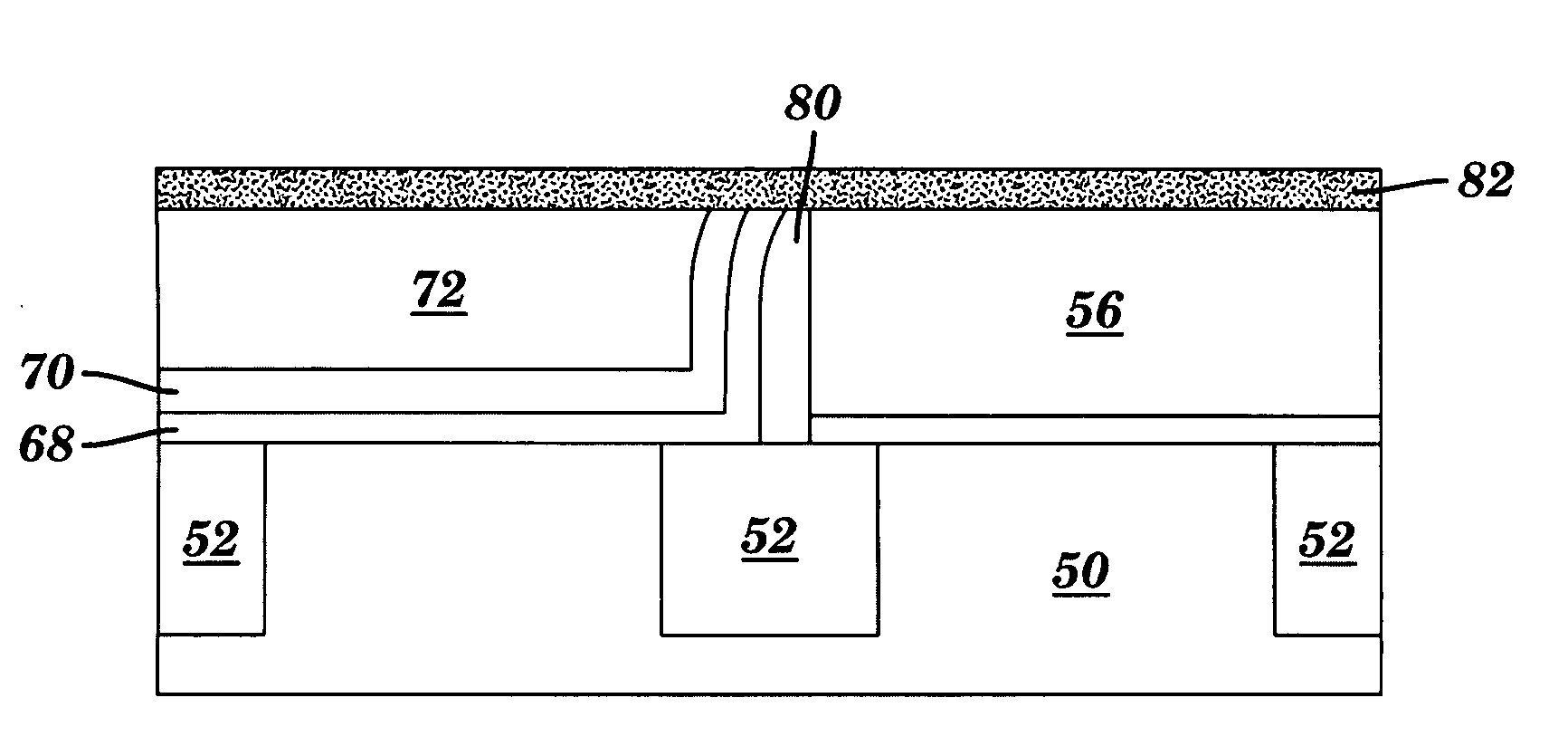
[0014]The fabrication of CMOS transistors with an air gap between the N-type and P-type doped regions of a gate electrode shared by the transistors is disclosed herein. This air gap serves to prevent or inhibit the cross-diffusion of dopants between the oppositely doped regions of the gate electrode. In the absence of such cross-diffusion, the distances between adjacent NFET and PFET devices can be reduced without being concerned that VT variations might occur and undesirably cause VT mismatch between the NFET and PFET devices. As such, more dense integrated circuits such as SRAM circuits can be formed without compromising the stability of such circuits.

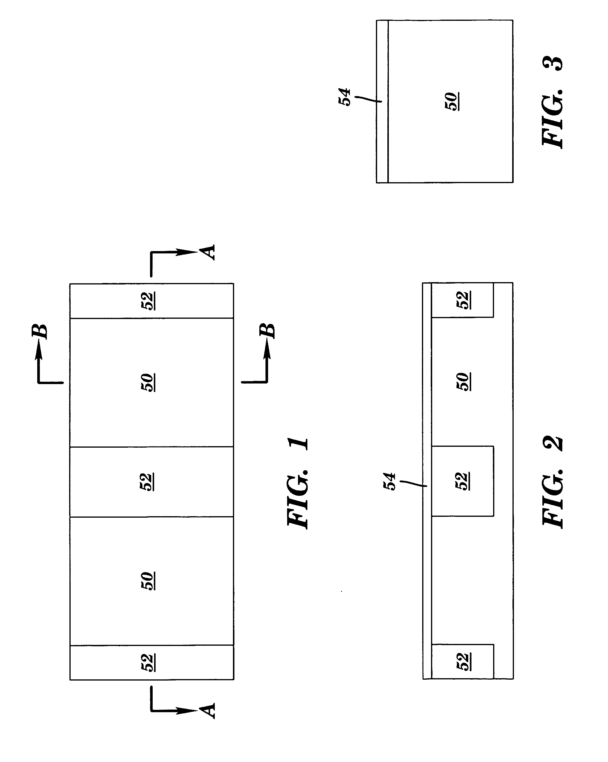
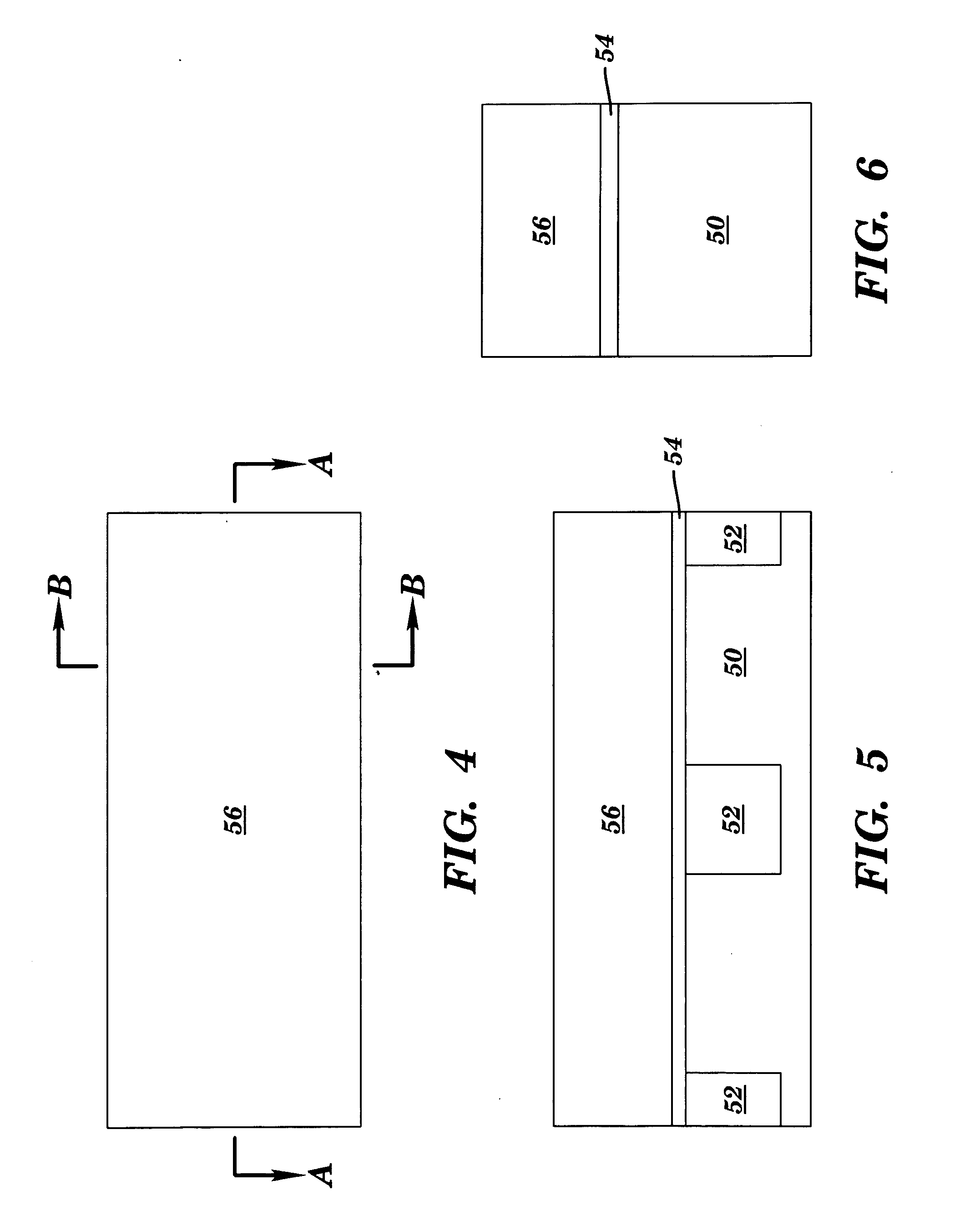
[0015]Turning now to the drawings in greater detail, it will be seen that FIGS. 1-27 illustrate an exemplary embodiment of a m...


PUM


Abstract

Stress enhanced transistor devices and methods of fabricating the same are provided. In one embodiment, a transistor device comprises: a gate conductor disposed above a semiconductor substrate between a pair of dielectric spacers, wherein the semiconductor substrate comprises a channel region underneath the gate conductor and recessed regions on opposite sides of the channel region, wherein the recessed regions undercut the dielectric spacers to form undercut areas of the channel region; and epitaxial source and drain regions disposed in the recessed regions of the semiconductor substrate and extending laterally underneath the dielectric spacers into the undercut areas of the channel region.

Description

BACKGROUND OF THE INVENTION[0001]1. Field of the Invention[0002]This invention relates to semiconductor fabrication, and particularly to fabricating CMOS transistor devices with an air gap between the N-type and P-type doped regions of a gate electrode for reducing threshold voltage variations that can be caused by dopant cross-diffusion.[0003]2. Description of Background[0004]Integrated circuits often employ active devices known as transistors such as field effect transistors (FETs). A metal-on-semiconductor field effect transistor (MOSFET) includes a silicon-based substrate comprising a pair of impurity regions, i.e., source and drain junctions, spaced apart by a channel region. A gate electrode is dielectrically spaced above the channel region of the silicon-based substrate. The junctions can comprise dopants which are opposite in type to the dopants residing within the channel region. MOSFETs comprising n-type doped junctions are referred to as NFETs, and MOSFETs comprising p-ty...

Claims


Application Information

Patent Timeline
IPC IPC(8): H01L21/8238H01L27/092
CPCH01L21/764H01L21/823842H01L29/517H01L21/823871H01L29/4966H01L21/823864
Inventor DYER, THOMAS W.YANG, HAINING S.
Owner GLOBALFOUNDRIES INC
Why Eureka
Try Eureka