
Liquid crystal display panel and method of fabricating the same

a technology of liquid crystal display panel and liquid crystal, which is applied in non-linear optics, instruments, optics, etc., can solve the problems of reducing productivity, increasing liquid crystal correspondingly, and vacuum injection method unable to cope with large-scale liquid crystal display panel

Active Publication Date: 2009-12-31
LG DISPLAY CO LTD
View PDF3 Cites 9 Cited by
  • Summary
  • Abstract
  • Description
  • Claims
  • Application Information

AI Technical Summary

Benefits of technology

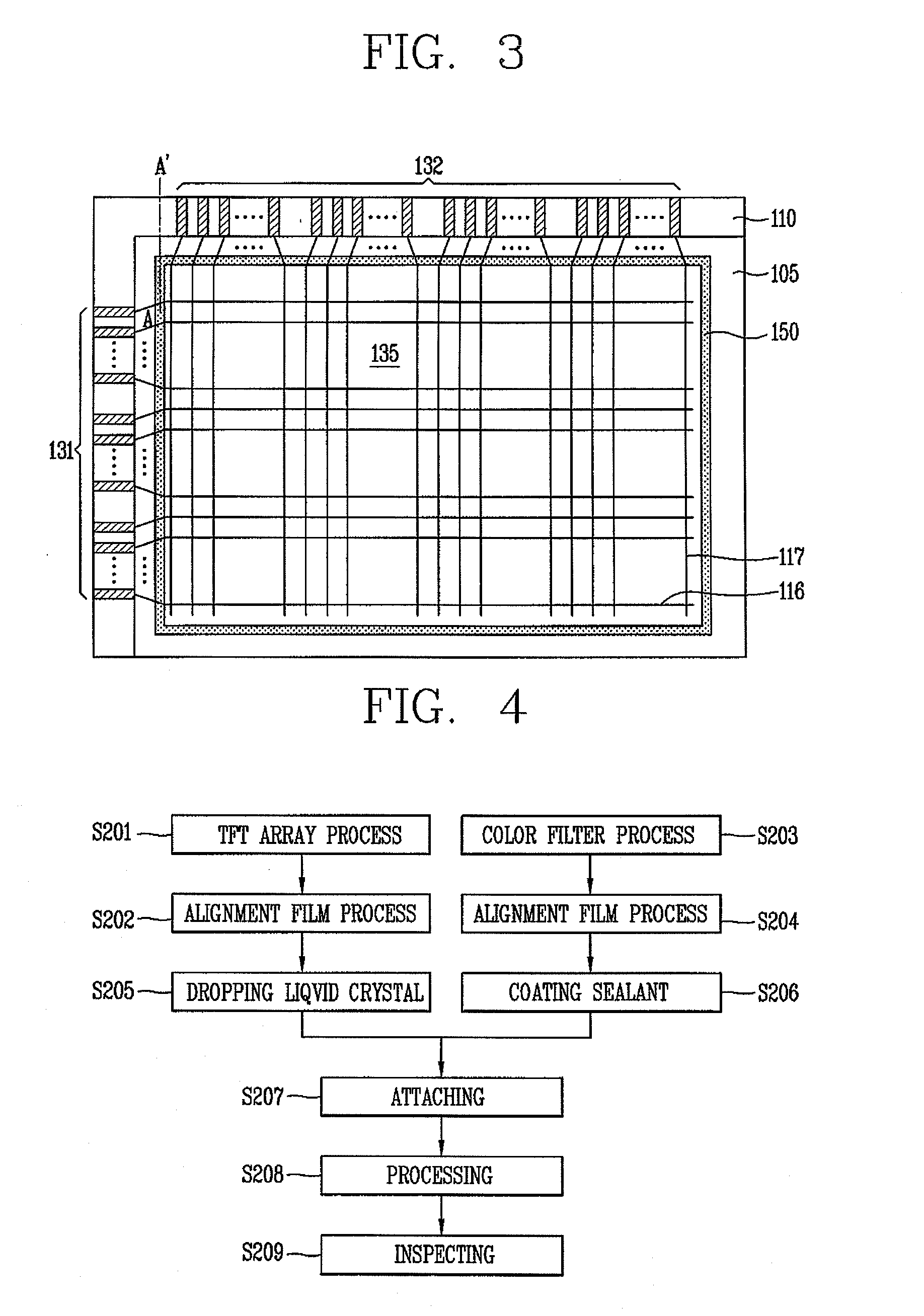
[0027]A method of fabricating a liquid crystal display panel according to the present invention comprises the steps of providing an array substrate having a pixel part and a color filter substrate; performing an array process in which thin film transistors are formed on the array substrate and a plurality of signal wires for transmitting signals to the thin film transistors are formed; performing a color filter process for forming color filters on the color filter substrate; and attaching the array substrate and the color filter substrate by dropping liquid crystal on to the array substrate or the color filter substrate and forming a seal line along an outer edge of the pixel part, wherein holes are formed within the signal wires passing through the seal line so as to have a different width at an inner side and an outer side of the liquid crystal display panel with respect to a predetermined region of the seal line.
[0027]A method of fabricating a liquid crystal display panel according to the present invention comprises the steps of providing an array substrate having a pixel part and a color filter substrate; performing an array process in which thin film transistors are formed on the array substrate and a plurality of signal wires for transmitting signals to the thin film transistors are formed; performing a color filter process for forming color filters on the color filter substrate; and attaching the array substrate and the color filter substrate by dropping liquid crystal on to the array substrate or the color filter substrate and forming a seal line along an outer edge of the pixel part, wherein holes are formed within the signal wires passing through the seal line so as to have a different width at an inner side and an outer side of the liquid crystal display panel with respect to a predetermined region of the seal line.
[0027]A method of fabricating a liquid crystal display panel according to the present invention comprises the steps of providing an array substrate having a pixel part and a color filter substrate; performing an array process in which thin film transistors are formed on the array substrate and a plurality of signal wires for transmitting signals to the thin film transistors are formed; performing a color filter process for forming color filters on the color filter substrate; and attaching the array substrate and the color filter substrate by dropping liquid crystal on to the array substrate or the color filter substrate and forming a seal line along an outer edge of the pixel part, wherein holes are formed within the signal wires passing through the seal line so as to have a different width at an inner side and an outer side of the liquid crystal display panel with respect to a predetermined region of the seal line.

Problems solved by technology

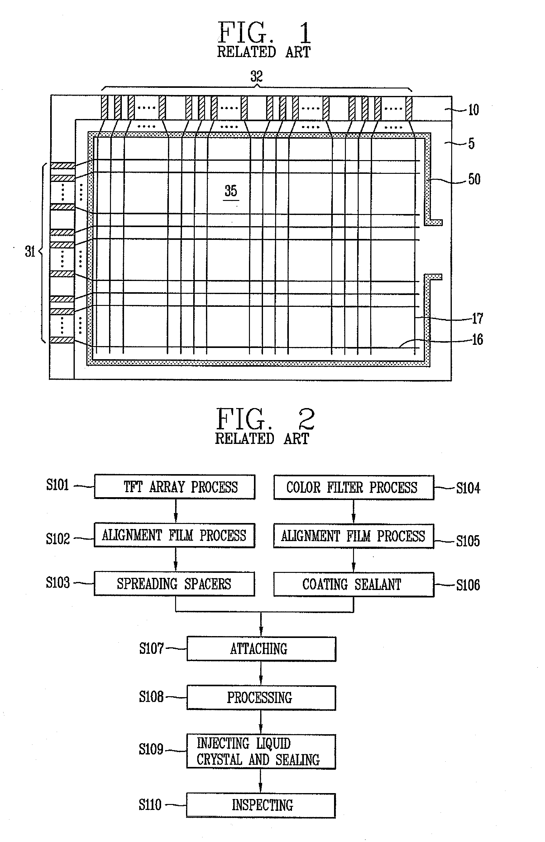
First, it takes a long time to fill the liquid crystal into the liquid crystal display panel. In general, the attached liquid crystal display panel with an area of several hundreds cm2 has a gap of a few micrometers (μm). Thus, even with the vacuum injection method, which uses pressure difference, an injecting amount of the liquid crystal by unit time is quite small. For instance, when fabricating a liquid crystal display panel of about 15 inches, it takes 8 hours to fill the liquid crystal display panel with liquid crystal. Therefore, because it takes such a long time to fabricate the liquid crystal display panel, productivity is decreased. In addition, as the liquid crystal display panel increases in size, the time required for filling liquid crystal correspondingly increases and deficiencies in filling the liquid crystal may occur. Therefore, the vacuum injection method can hardly cope with a large-scale liquid crystal display panel.
Second, with the vacuum injection method, too much liquid crystal is consumed. In general, the actual injected quantity of liquid crystal in the vacuum injection method is very small compared to the quantity of liquid crystal filled in the container. When liquid crystal is exposed in the air or to a specific gas, it reacts with the gas and degrades. Thus, even if liquid crystal in a container is filled into a plurality of liquid crystal display panels, a large quantity of liquid crystal remaining after the filling has to be discarded, thereby increasing the overall unit price of the liquid crystal display and decreasing price competitiveness.

Method used


Image

  • Liquid crystal display panel and method of fabricating the same
  • Liquid crystal display panel and method of fabricating the same
  • Liquid crystal display panel and method of fabricating the same

Examples


first embodiment

[0070]FIGS. 5A and 5B are views schematically showing a wiring structure according to the present invention. FIG. 5A shows a case where signal wires pass through the seal line in a vertical direction, and FIG. 5B shows a case where the signal wires pass through the seal line in an oblique direction.

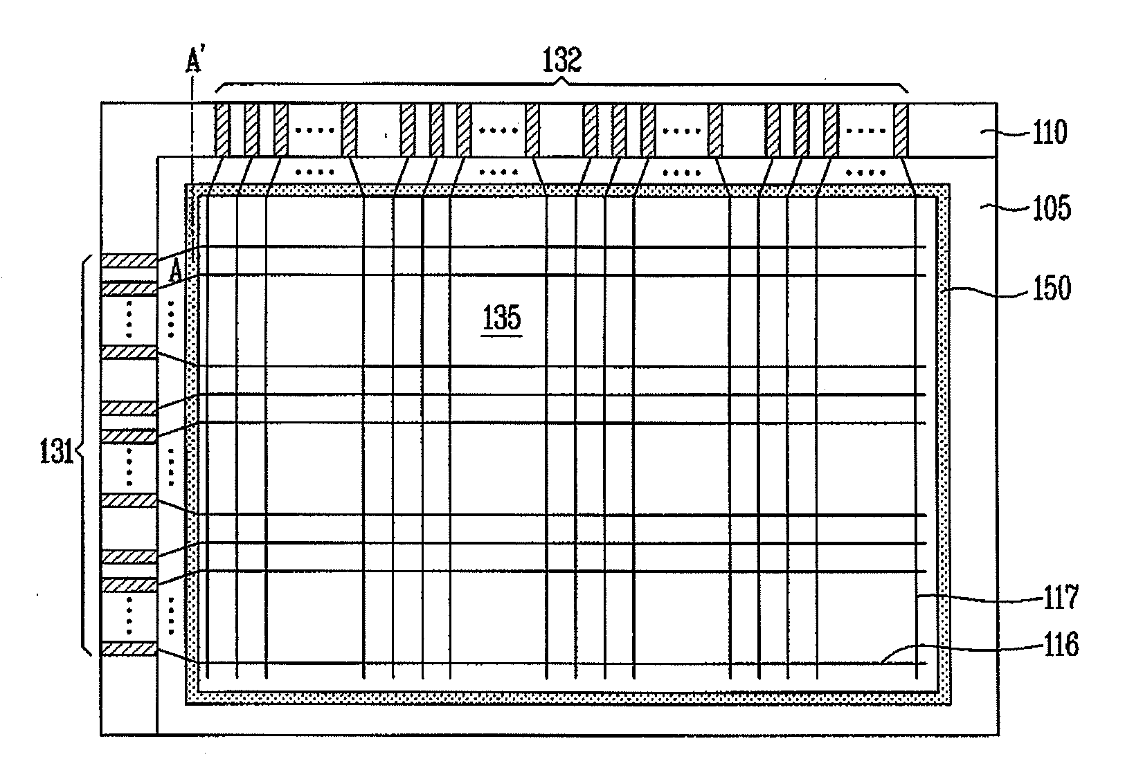
[0071]FIG. 6 is a cross sectional view taken along line A-A′ of the structure of the liquid crystal display panel as shown in FIG. 3.

[0072]As shown therein, a color filter substrate 105 and an array substrate 110 according to the first embodiment of the present invention are attached by a seal line 150, with liquid crystal (not shown) dropped thereon, to constitute the liquid crystal display panel.

[0073]At this time, predetermined signal wires 120 pass through part of the seal line 150 in order to transmit a signal to a pixel part of the liquid crystal display panel from a driving unit. Predetermined holes 125 are formed within the wires 120 passing through the seal line 120 and filled wi...

second embodiment

[0079]FIG. 7 is a view schematically showing a wiring structure according to the present invention.

[0080]As shown therein, a color filter substrate 205 and an array substrate 210 according to the second embodiment of the present invention are attached by a seal line 250, with liquid crystal (not shown) dropped thereon, to constitute the liquid crystal display panel.

[0081]At this time, predetermined signal wires 220 pass through part of the seal line 250 in order to transmit a signal to a pixel part of the liquid crystal display panel from a driving unit. Predetermined holes 225a and 225b are formed within the wires 220 passing through the seal line 250 and filled with a sealant, thereby increasing the attachment force between the color filter substrate 205 and the array substrate 210.

[0082]In the second embodiment of the present invention, the width and length of the holes 225a and 225b are designed differently at an inner side and an outer side of the liquid crystal display panel w...

third embodiment

[0089]As shown therein, a color filter substrate 305 and an array substrate 310 according to the present invention are attached by a seal line 350, with liquid crystal (not shown) dropped thereon, to constitute the liquid crystal display panel.

[0090]At this time, predetermined signal wires 320 pass through part of the seal line 350 in order to transmit a signal to a pixel part of the liquid crystal display panel from a driving unit. Predetermined holes 325a and 325b are formed within the wires 320 passing through the seal line 350 and filled with a sealant, thereby increasing the attachment force between the color filter substrate 305 and the array substrate 310.

[0091]In the third embodiment of the present invention, the width and length of the holes 325a and 325b are designed differently at an inner side and an outer side of the liquid crystal display panel with respect to a predetermined region of the seal line in the same manner as in the second embodiment. Thus, the resistance o...


PUM


Abstract

Provided are a liquid crystal display panel and a method of fabricating the same, which can increase the attachment force of the liquid crystal display panel by forming holes in wires passing through a seal line in a case where a liquid crystal layer is formed by a dropping method, reduce the resistance of the wires by differentiating the width of the holes from the width of the wires with respect to a specific region of the seal line, and prevent an afterimage defect caused by blurring and contamination of the seal line.The liquid crystal display panel comprises: an array substrate having a pixel part and a color filter substrate; a seal line formed along an outer edge of the pixel part to attach the array substrate and the color filter substrate together; a plurality of signal wires for transmitting signals to the pixel part; and holes formed within the signal wires passing through the seal line and filled with a sealant comprising the seal line, wherein the holes are designed to have a different width at an inner side and an outer side of the liquid crystal display panel with respect to a predetermined region of the seal line.

Description

RELATED APPLICATION[0001]The present disclosure relates to subject matter contained in priority Korean Application No. 10-2008-0060424, filed on Jun. 25, 2008, which is herein expressly incorporated by reference in its entirety. federally sponsored research or developmentBACKGROUND[0002]1. Field of the Disclosure[0003]The present invention relates to a liquid crystal display panel and a method of fabricating the same, and particularly, to a liquid crystal display panel, which has a liquid crystal layer formed by a dropping method, and a method of fabricating the same.[0004]2. Description of the Related Art[0005]In general, the LCD device is a display device in which data signals corresponding to image information is supplied to a matrix of pixels. The data signals control optical transmittance of the pixels so as to display images.[0006]The LCD device includes a liquid crystal display panel in which the pixels are arranged in a matrix and a driving part for driving the pixels.[0007]...

Claims


Application Information

Patent Timeline
IPC IPC(8): G02F1/1339G02F1/1343G02F1/1333
CPCG02F1/1345G02F1/1339
Inventor KWON, JAO-CHANGSHIM, YU-RISHIN, CHANG-YEOPOH, CHUNG-WANKIM, DONG-BOK
Owner LG DISPLAY CO LTD
Learn More