CMOS transistor and the method for manufacturing the same

a transistor and cmos technology, applied in the field of cmos transistors, can solve the problems of silicide agglomeration that increases resistance, and the method has encountered difficulties with high-expense and technical bottlenecks, and achieve the effect of preventing ge-out diffusion

Inactive Publication Date: 2010-01-07
UNITED MICROELECTRONICS CORP
View PDF6 Cites 67 Cited by
  • Summary
  • Abstract
  • Description
  • Claims
  • Application Information

AI Technical Summary

Benefits of technology

[0008]In order to overcome the issue of Ge-out diffusion, the present invention provides a method of manufacturing a CMOS transistor, which is capable of preventing Ge-out diffusion. Initially, a semiconductor substrate having at least a PMOS transistor and an NMOS transistor is provided. The source/drain of the PMOS transistor h...

Problems solved by technology

However, this method has encountered difficulties with high-expenses and technical bottlenecks in recent years.
The substrate-strained based system is performed with a strained-silicon substrate or a selective epitaxial growth process that results in ...

Method used


Image

  • CMOS transistor and the method for manufacturing the same
  • CMOS transistor and the method for manufacturing the same
  • CMOS transistor and the method for manufacturing the same

Examples


Embodiment Construction

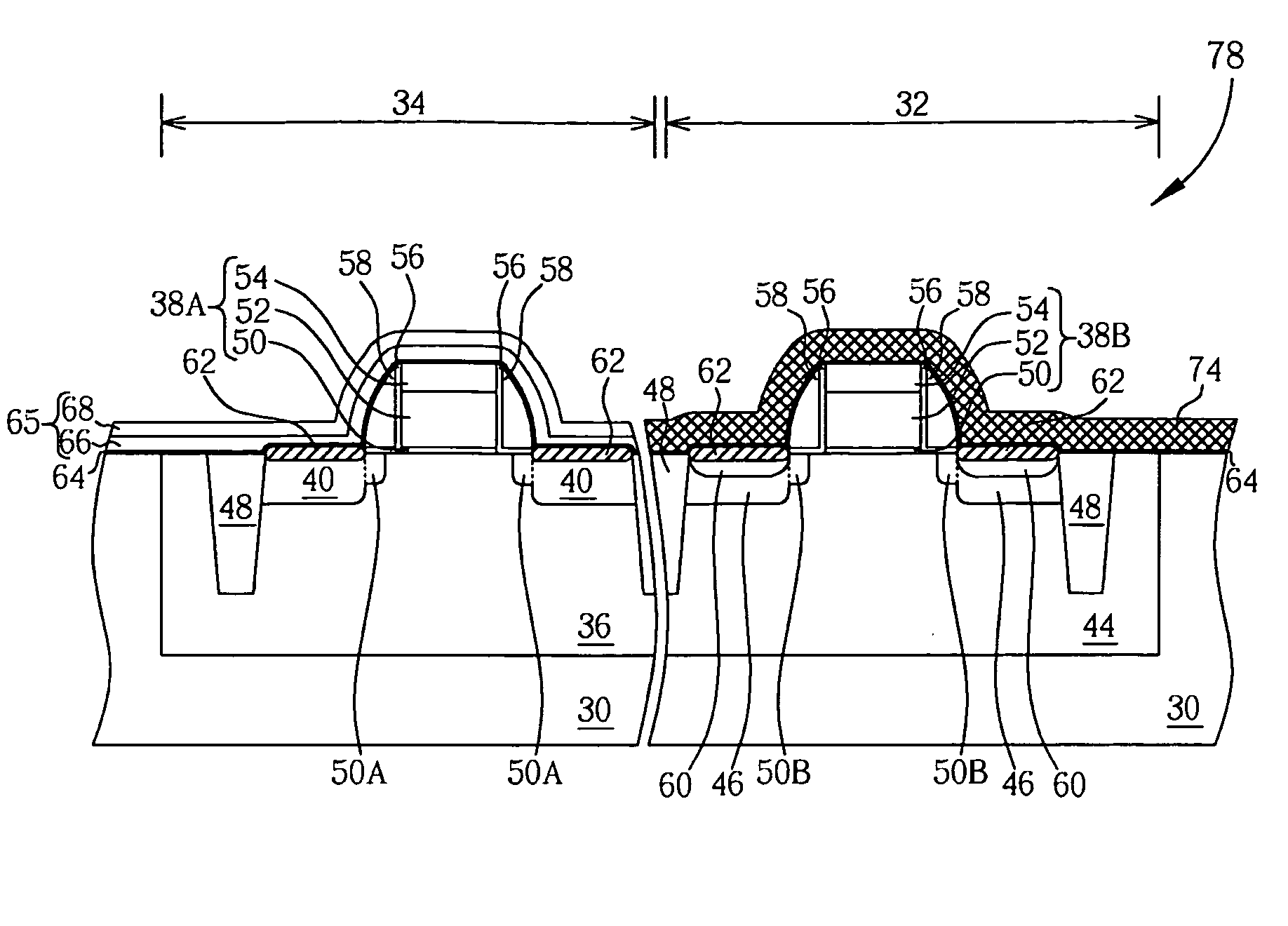
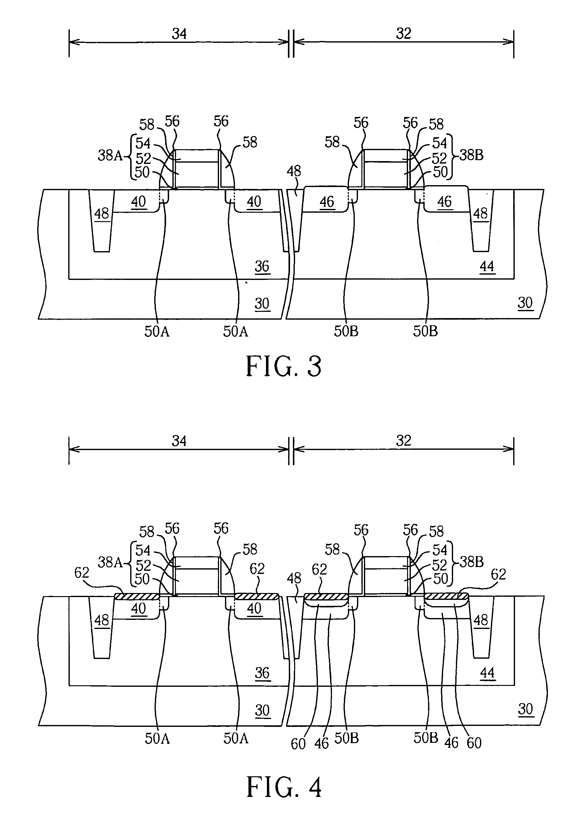
[0017]Please refer to FIG. 3 through FIG. 10. FIG. 3 to FIG. 9 are schematic diagrams illustrating a method for manufacturing a CMOS transistor according to a preferred embodiment of the present invention. FIG. 10 is a flow diagram of the method of the present invention to manufacture the CMOS transistor for preventing Ge-out diffusion. Please refer to FIG. 3. A semiconductor substrate 30 is provided, in which the semiconductor substrate 30 has at least a PMOS transistor 32 and an NMOS transistor 34 disposed thereon. The NMOS transistor 34 is formed in a P well 36 disposed in the semiconductor substrate 30. The NMOS transistor 34 includes a gate structure 38A formed on the surface of the semiconductor substrate 30 and a source / drain 40 disposed beside the gate structure 38A. The PMOS transistor 32 is formed in an N well 44. The PMOS transistor 32 includes a gate structure 38B formed on the surface of the semiconductor substrate 30 and a source / drain 46 disposed beside the gate struc...


PUM


Abstract

A CMOS transistor and a method for manufacturing the same are disclosed. A semiconductor substrate having at least a PMOS transistor and an NMOS transistor is provided. The source/drain of the PMOS transistor comprises SiGe epitaxial layer. A carbon implantation process is performed to form a carbon-doped layer in the top portion of the source/drain of the PMOS transistor. A silicide layer is formed on the source/drain. A CESL is formed on the PMOS transistor and the NMOS transistor. The formation of the carbon-doped layer is capable of preventing Ge out-diffusion.

Description

BACKGROUND OF THE INVENTION[0001]1. Field of the Invention[0002]The present invention is related to a CMOS transistor and a method for manufacturing the same, and particularly, to a CMOS transistor capable of preventing Ge out-diffusion and a method for manufacturing the same.[0003]2. Description of the Prior Art[0004]Industrial circles are used to reducing device dimensions to improve the performance of metal-oxide semiconductor (MOS) transistors. However, this method has encountered difficulties with high-expenses and technical bottlenecks in recent years. For these reasons, the industrial circles seek other methods to improve MOS transistor performance. And accordingly, a popular method is to utilize the material characteristics to cause strain effect on MOS transistors.[0005]In order to increase the driving current of a complementary metal-oxide semiconductor (CMOS) transistor including a p-type MOS (PMOS) transistor and an n-type MOS (NMOS) transistor, the industrial circles de...

Claims


Application Information

Patent Timeline
IPC IPC(8): H01L21/8238H01L27/092
CPCH01L21/26506H01L21/823807H01L29/7843H01L29/165H01L29/66628H01L21/823814H01L21/26513
Inventor CHEN, YI-WEITSAI, TENG-CHUNHUANG, CHIEN-CHUNGCHEN, JEI-MINGHSIAO, TSAI-FU
Owner UNITED MICROELECTRONICS CORP
Why Eureka
Try Eureka