Semiconductor device and method of manufacturing thereof

a technology of semiconductor devices and semiconductors, applied in semiconductor devices, semiconductor/solid-state device details, electrical apparatus, etc., can solve problems such as increasing the resistance of conductive structures, and achieve the effect of reducing the resistance of conductors

Inactive Publication Date: 2010-01-07
NXP BV
View PDF18 Cites 409 Cited by
  • Summary
  • Abstract
  • Description
  • Claims
  • Application Information

AI Technical Summary

Benefits of technology

[0010]The object of the invention is realized in that a semiconductor device in accordance with the opening paragraph is provided, which is characterized in that the first top surface coincides with the second top surface, and in that the airgaps extend from the surface of the body to said first and second top surface. The invention is based upon the insight that the problem resulting from a misalignment in a via which has to land on the conductor (unlanded via) can be solved with the spacers themselves. This can be done by making the spacers extend to the top of the conductor while at the same time making the airgaps extend to the top surface of the spacer and the conductor. This combination of features excludes the possibility of a capping layer that extends to below the top surface of the conductor. Above that, such capping layer is not needed anymore. The combination of all mentioned features further makes the conductor benefit fully from the vertical space available in the insulating layer, which on its turn allows for a larger cross-sectional area of the conductor at a specific interconnect width. A larger cross-sectional area implies a lower interconnect resistance and thus the object of the invention is achieved.
[0033]Preferably, the insulating sidewall spacers are provided with a width that lies between 5% and 40% of the width of the conductor. Such a range provides a convenient tolerance for unlanded vias while still enabling a small pitch between neighboring conductors (which is beneficial for the packing density).

Problems solved by technology

A drawback of the known semiconductor device is that at a specific width of the conductor the cross-sectional area available for the conductor is significantly reduced by the required additional capping layer, which results in an increased resistance of the conductive structure.

Method used


Image

  • Semiconductor device and method of manufacturing thereof
  • Semiconductor device and method of manufacturing thereof
  • Semiconductor device and method of manufacturing thereof

Examples


first embodiment

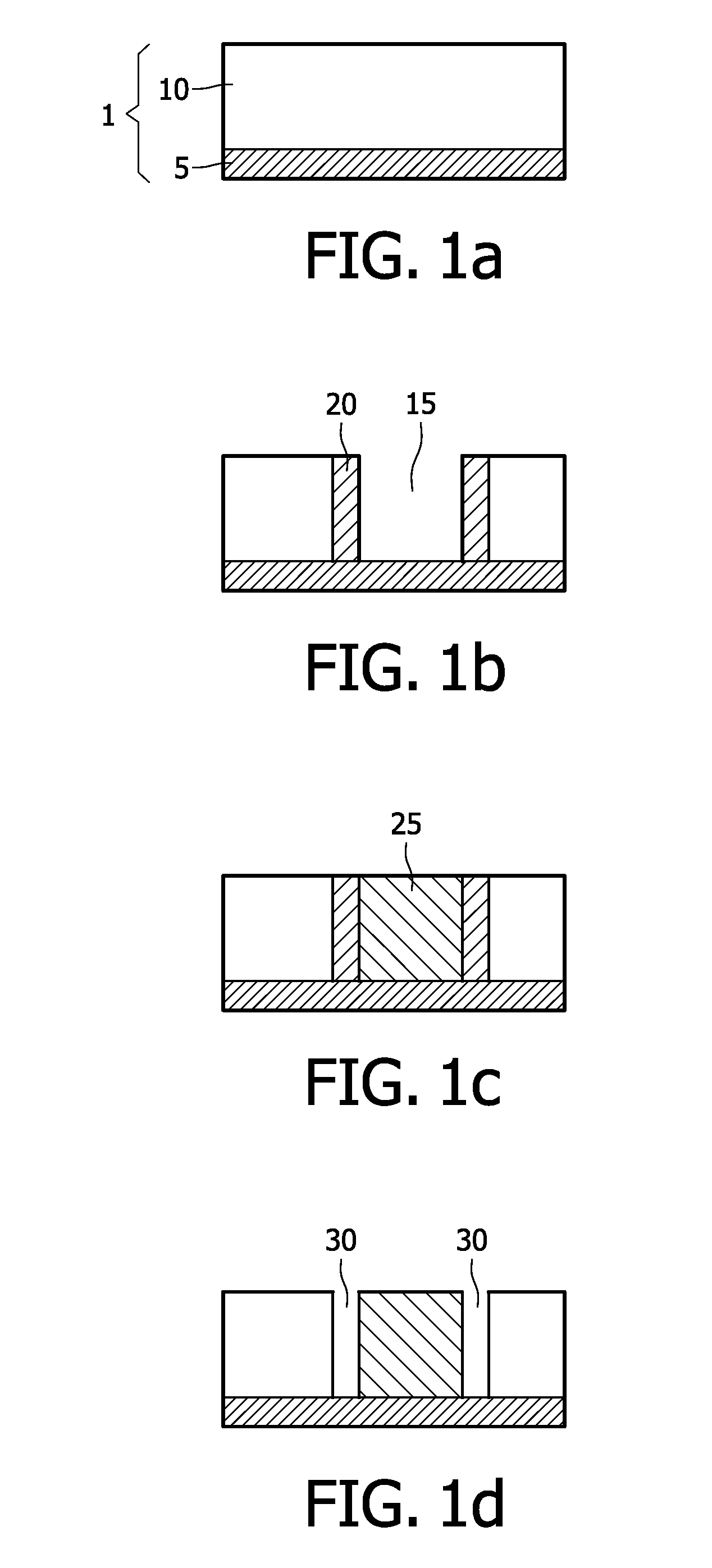
[0060]FIGS. 4a to 4h illustrate the method of manufacturing a semiconductor device according to the invention. This embodiment will be mainly discussed as far as it differs from the known method as illustrated in FIGS. 1a to 1f.

[0061]The stage of the method according to the invention as illustrated in FIG. 4a is similar to the stage of the known method in FIG. 1a.

[0062]The stage of the method according to the invention as illustrated in FIG. 4b is similar to the stage of the known method in FIG. 1b.

[0063]Referring to FIG. 4c, in this stage an insulating spacer layer 21 is provided on the insulating layer 10 and on all walls of the opening 15. The thickness of this insulating spacer layer 21 determines the width of the insulating sidewall spacers 22 which will be formed later. The insulating spacer layer 21 can be provided using conventional deposition techniques like CVD, ALD, spin-on coating etc. Referring to FIG. 4d, in this stage the insulating sidewall spacers 22 are formed b...

second embodiment

[0071]Various variations of the method are possible. The first and the method can even be combined without any problems.

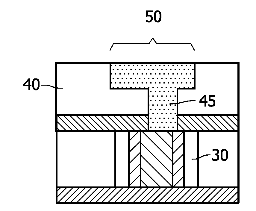
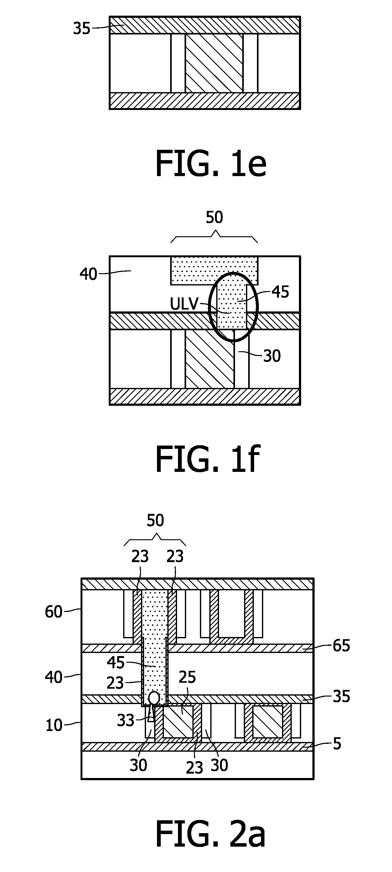
[0072]Although the given examples in FIGS. 1f, 4h and 5g present a dual-damascene interconnect layer 40, 45, 50, the invention can be easily applied in single-damascene processes as well.

[0073]Also, the invention is applicable in both complete airgap configurations, as well as partial airgap configurations. One way of creating full airgap configurations is to implement the insulating layer 10 as a fully as a sacrificial layer.

[0074]As an alternative to the methods illustrated in FIGS. 4a to 4h and FIGS. 5a to 5g it is also possible to provide the sacrificial regions 20 (or the complete insulating layer, when complete airgaps are desired) as a thermal degradable material. The formation of the airgaps 30 may then be done by thermal degradation of the thermodegradable material.

[0075]The invention thus provides a semiconductor device comprising:[0076]a substrate, the s...


PUM


Abstract

The invention relates to a semiconductor device comprising: a substrate (1), the substrate (1) comprising a body (5), the body (5) having a surface, the substrate (1) being provided with an insulating layer (10) on the surface of the body (1);—a conductor (25) with insulating sidewall spacers (22) located in the insulating layer (10), the conductor (25) having a current-flow direction during operation, the conductor (25) having a first width, the insulating sidewall spacers (22) each having a second width being smaller than the first width of the conductor (25), the first width and the second width being measured in a direction perpendicular to the current-flow direction of the conductor (25) and parallel to said surface, the conductor (25) having a first top surface extending parallel to said surface, the insulating sidewall spacers (22) having a second top surface, and airgaps (30) located in the insulating layer (10) adjacent to the insulating sidewall spacers (22), characterized in that the first top surface coincides with the second top surface, and in that the airgaps (30) extend from the surface of the body (5) to said first and second top surface. The invention further relates to a method of manufacturing such a semiconductor device. The semiconductor device according to the invention enables a lower resistance of the conductor while still providing a tolerance for unlanded vias.

Description

FIELD OF THE INVENTION[0001]The invention relates to semiconductor device comprising:[0002]a substrate, the substrate comprising a body, the body having a surface, the substrate being provided with an insulating layer on the surface of the body;[0003]a conductor with insulating sidewall spacers located in the insulating layer, the conductor having a current-flow direction during operation, the conductor having a first width, the insulating sidewall spacers each having a second width being smaller than the first width of the conductor, the first width and the second width being measured in a direction perpendicular to the current-flow direction of the conductor and parallel to said surface, the conductor having a first top surface extending parallel to said surface, the insulating sidewall spacers having a second top surface, and[0004]airgaps located in the insulating layer adjacent to the insulating sidewall spacers.[0005]The invention further relates to a method of manufacturing su...

Claims


Application Information

Patent Timeline
Patent Type & Authority Applications(United States)
IPC IPC(8): H01L23/48H01L21/768H01L23/522
CPCH01L21/7682H01L21/76825H01L2924/09701H01L23/5222H01L23/53295H01L21/76831H01L2924/0002H01L2221/1063H01L2924/00
Inventor HUMBERT, AURELIEHOOFMAN, ROMANO
Owner NXP BV
Why Eureka
Try Eureka