Electrical insulating layers, UV protection, and voltage spiking for electro-active diffractive optics

a technology of electrical insulation layer and voltage spiking, applied in the field of electrical insulation layer, uv protection, voltage spiking of electro-active diffractive optics, can solve the problems of quadratic switching time between different states of electro-active materials, unable to achieve the effect of electrical conduction

Inactive Publication Date: 2010-01-07
PIXELOPTICS
View PDF6 Cites 54 Cited by
  • Summary
  • Abstract
  • Description
  • Claims
  • Application Information

AI Technical Summary

Benefits of technology

[0014]In another embodiment of the present invention an electro-active lens has a first substrate having a surface relief diffractive topological profile forming a plurality of peaks. A second substrate having a substantially smooth topological profile is positioned facing the surface relief diffractive topological profile. A first electrode and a second electrode is disposed between the substrates following the topological profiles of the first and second substrates, respectively. The electrodes form a gap between the substrates narr

Problems solved by technology

Such matching results in a canceling out of the optical power of the diffractive optic.
Using electro-active material, however, presents problems.
One problem is that the switching times between different states of the electro-active material is quadratic with respect to the material's thickness.
However, by narrow

Method used


Image

  • Electrical insulating layers, UV protection, and voltage spiking for electro-active diffractive optics
  • Electrical insulating layers, UV protection, and voltage spiking for electro-active diffractive optics
  • Electrical insulating layers, UV protection, and voltage spiking for electro-active diffractive optics

Examples


Embodiment Construction

[0022]The following preferred embodiments as exemplified by the drawings are illustrative of the invention and are not intended to limit the invention as encompassed by the claims of this application.

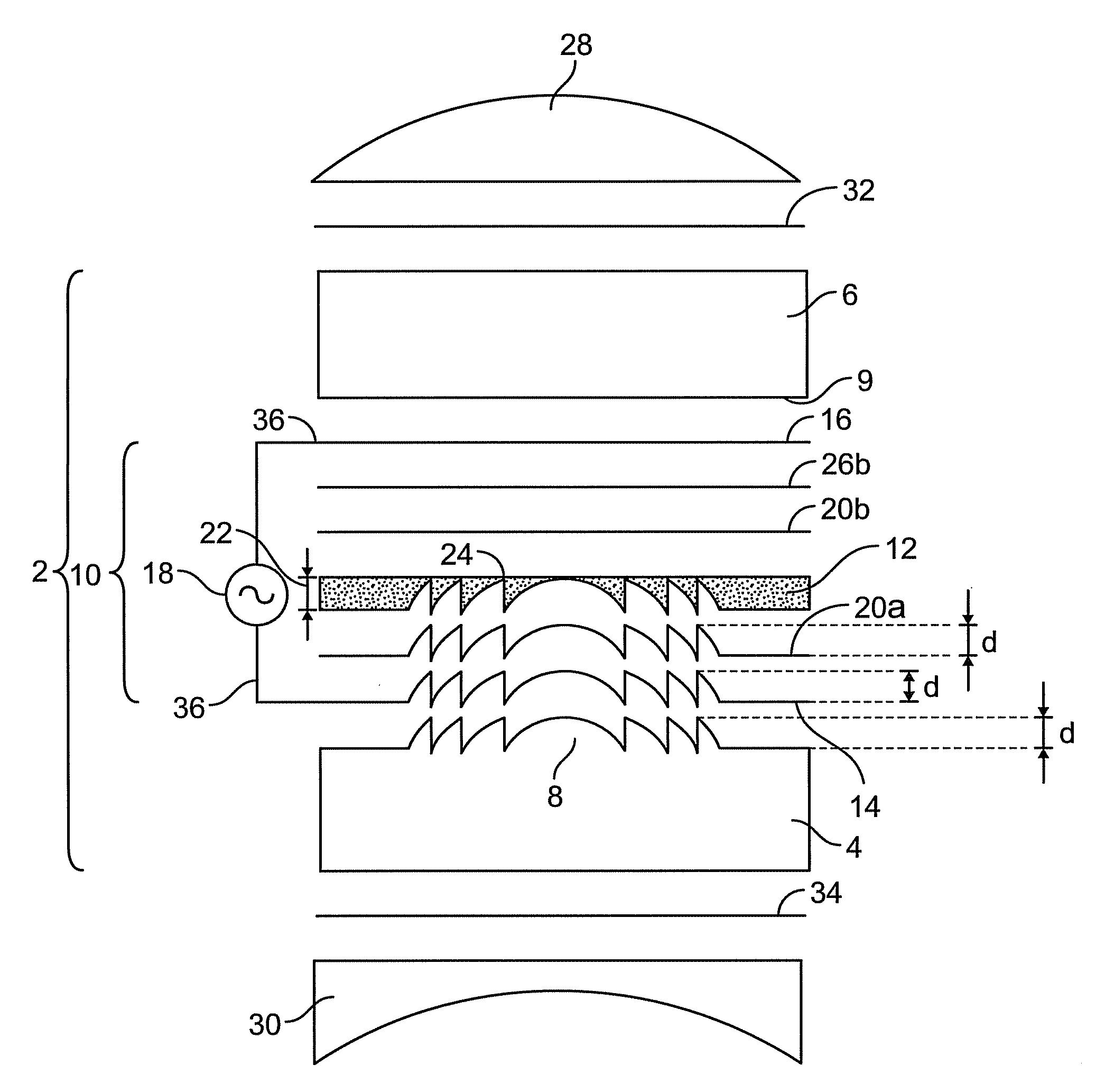
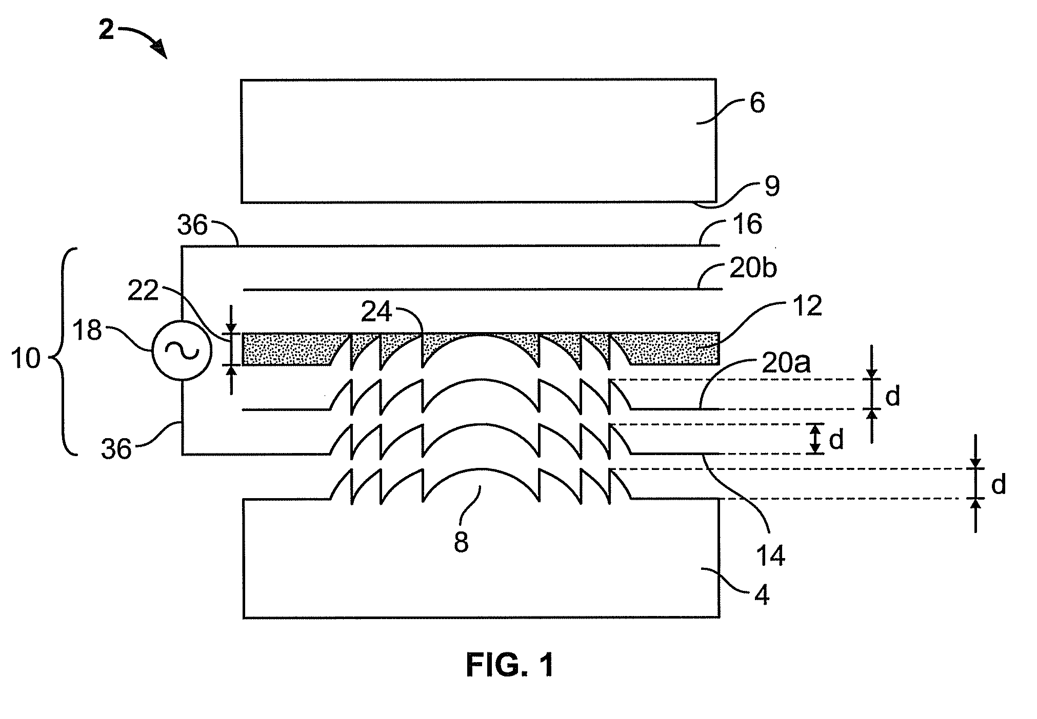
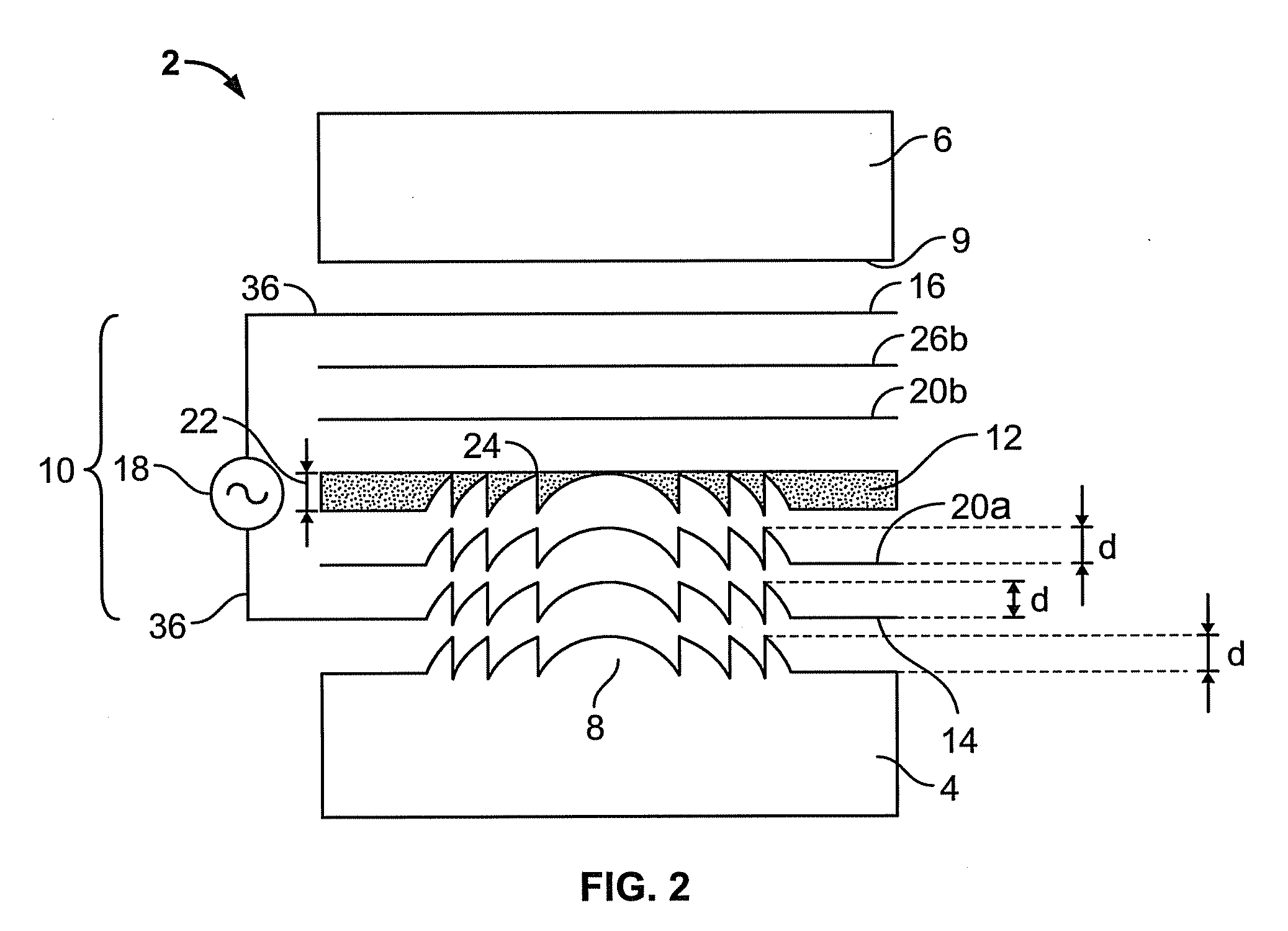
[0023]FIG. 1 shows a schematic side view drawing of an electro-active lens 2. The electro-active lens may include a first substrate 4 and a second substrate 6 positioned on opposite sides of the lens. The first substrate may have a surface relief diffractive topological profile 8 for diffracting light. The surface relief diffractive pattern may vary along a maximum thickness, d. The second substrate may have a substantially smooth topological profile 9. The smooth topological profile of substrate 6 faces the surface relief diffractive profile of substrate 4. Each of the substrates may have fixed optical properties, such as a refractive index (n) approximately equal to 1.67. The substrates may be composed of materials including, for example, A09 (manufactured by Brewer Science, having n=...


PUM


Abstract

An electro-active lens has a first substrate with a surface relief diffractive topological profile and a second substrate positioned opposite to the first substrate having a substantially smooth topological profile. A first electrode is positioned along the surface relief diffractive topological profile of the first substrate and a second electrode is positioned between the first electrode and the second substrate. The smallest distance between the electrodes is less than or equal to about 1 micron An electro-active material is positioned between the first and second electrodes and a first insulating layer is positioned between the first and second electrodes.

Description

CROSS REFERENCE TO RELATED APPLICATIONS[0001]This application claims priority from and incorporates by reference in their entirety the following U.S. provisional applications:[0002]U.S. Provisional Application Ser. Nos. 60 / 906,211, filed on 12 Mar. 2007 and 60 / 971,308, filed on 11 Sep. 2007, both entitled “Electrical Insulating Layers, UV Protection, and Voltage Spiking for Electro-Active Diffractive Optics” and U.S. Provisional Application Ser. No. 60 / 974,504, filed on 24 Sep. 2007 entitled, “Electro-active Diffractive Lens With Self Regulated Thickness of Electro-active Material.FIELD OF THE INVENTION[0003]The present invention relates to reducing the thickness of an electro-active element in an ophthalmic lens while preventing electrical conduction between electrodes by providing insulating material between electrodes.BACKGROUND OF THE INVENTION[0004]An electro-active lens is a device that has alterable optical properties, such as focal length, opacity, etc. The alterable optical...

Claims


Application Information

Patent Timeline
IPC IPC(8): G02C7/06G02F1/29G02F1/1335
CPCG02C7/101G02F2001/294G02F1/29G02F1/133371G02F1/294G02C7/00G02C7/02
Inventor CLARKE, ROGERKOKONASKI, WILLIAMHADDOCK, JOSHUA N.IYER, VENKATRAMANI S.
Owner PIXELOPTICS
Why Eureka
Try Eureka