Photovoltaic devices inspection apparatus and method of determining defects in photovoltaic device

a technology of photovoltaic devices and inspection apparatus, which is applied in the direction of photovoltaic monitoring, instruments, material analysis, etc., can solve the problem that the photovoltaic device cannot be inspected in a production line, and achieve the effect of simple distinction, improved quality and durability, and easy and accurate determination

Inactive Publication Date: 2010-01-07
HISSHINBO HOLDINGS INC
View PDF3 Cites 18 Cited by
  • Summary
  • Abstract
  • Description
  • Claims
  • Application Information

AI Technical Summary

Benefits of technology

[0031]According to the photovoltaic devices inspection apparatus and the method of determining a defect of a photovoltaic devices of the present invention, bright and dark regions of a photographed cell image are displayed by enhancing the bright and dark regions through binarization, so that the bright and dark regions can be simply distinguished, and whether the bright and dark regions are defective can be easily and accurately determined.
[0032]Furthermore, photovoltaic device defects are classified into several types, and a region suspected to be a defect is compared with stored defect types, so that exact defect determination is possible. In addition, since a shape or size threshold value can be changed according to the defect types, defect determination can be performed according to actual situations. In addition, since it can be determined whether a defect grows or not according to the type of the defect in the future, a potential defect as well as a current defect can be determined. Therefore, photovoltaic devices having improved quality and durability can be provided.
[0033]In addition, particular types of defects, such as small cracks, are easily formed in the vicinity of busbars of a photovoltaic cell and may not be problematic in other regions of the photovoltaic cell. Such types of defects can also be appropriately detected according to the present invention. For example, in the case of detecting small cracks at a position distant from a busbar as well as a position adjacent to the busbar, a non-defective dark region caused by a boundary of crystals can be detected as a crack. Therefore, it is desirable that detection of a small crack is not performed for a region distant from a busbar.

Problems solved by technology

However, according to the method disclosed in Patent Document 3, photovoltaic devices cannot be inspected in a production line because it takes much time to change the temperature of the photovoltaic devices.

Method used


Image

  • Photovoltaic devices inspection apparatus and method of determining defects in photovoltaic device
  • Photovoltaic devices inspection apparatus and method of determining defects in photovoltaic device
  • Photovoltaic devices inspection apparatus and method of determining defects in photovoltaic device

Examples


Embodiment Construction

[0047]A detailed description will now be given of illustrative embodiments of the present invention, with reference to the accompanying drawings. In so doing, specific terminology is employed solely for the sake of clarity, and the present disclosure is not to be limited to the specific terminology so selected. It is to be understood that each specific element includes all technical equivalents that operate in a similar manner and achieve a similar result.

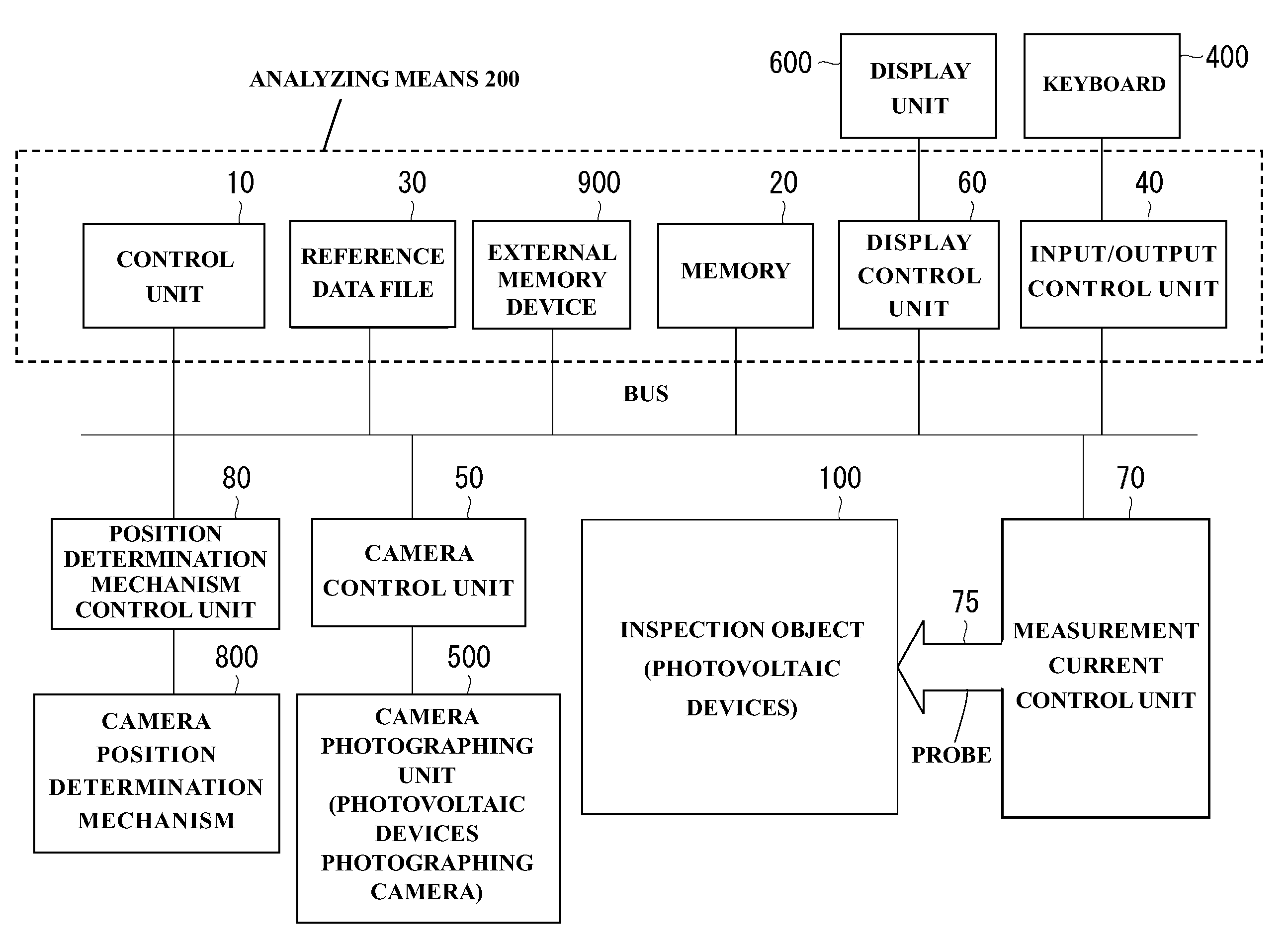
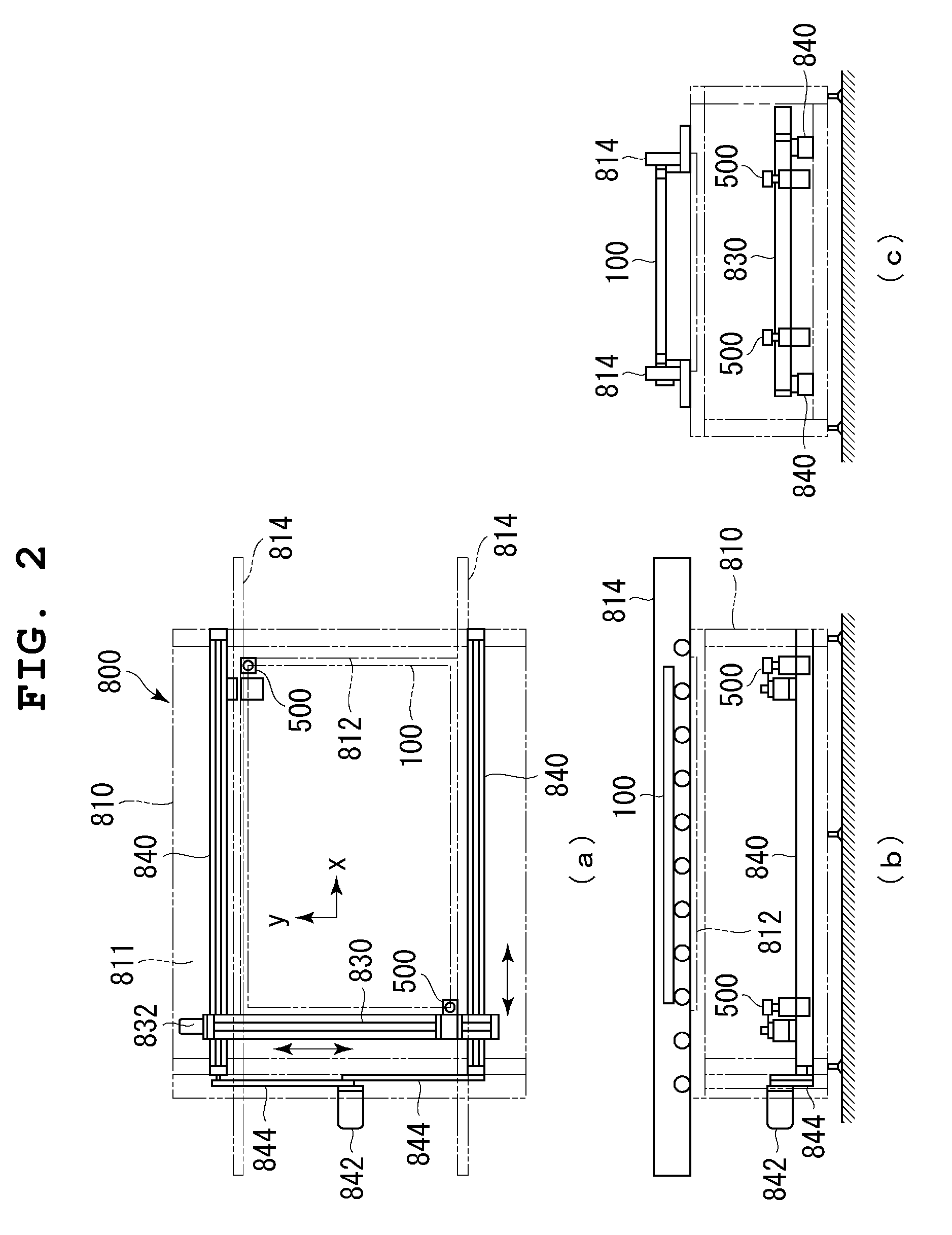
[0048]FIG. 1 is a block diagram illustrating a schematic configuration of a photovoltaic device inspection apparatus according to an embodiment of the present invention, and FIGS. 2A to 2C are views illustrating the configuration of a camera position determination mechanism of the apparatus of the embodiment, where FIG. 2A is a plan view, FIG. 2B is a front view, and FIG. 2C is a right side view. FIG. 3 is a flowchart for explaining a method of inspecting a photovoltaic device according to the embodiment; FIG. 4 is a flowchart for ...


PUM


Abstract

A photovoltaic devices inspection apparatus and method of determining defects in photovoltaic devices that uses electroluminescence can find both the quality of the photovoltaic devices from the state of electroluminescence and the possibility of the photovoltaic devices becoming defective in the future by applying constant electric current to the photovoltaic devices causing electroluminescence of the photovoltaic devices (S7), photographing the light emitted from each photovoltaic cell of the photovoltaic devices (S10), dividing the photographed image of the photovoltaic cell into a bright region and dark region by using a threshold value and displayed as an enhanced image by binarization, analyzing as classifying each photovoltaic cell defect according to defect types and comparing a shape of the dark region with the defect types (S50), determining the existence of the defect to perform a positive-negative quality judgment on the photovoltaic devices, and displaying images of the problematic regions for visual inspection (S16).

Description

CLAIM FOR PRIORITY[0001]The present specification claims priority from Japanese Patent Application No. 2008-171925, filed on Jul. 1, 2008 in the Japan Patent Office, the entire contents of which are hereby incorporated by reference herein.BACKGROUND OF THE INVENTION[0002]1. Field of the Invention[0003]The present invention relates to photovoltaic devices inspection apparatus configured to inspect a photovoltaic device that includes at least one photovoltaic cell and a method of determining defects in photovoltaic devices.[0004]2. Description of the Background Art[0005]It is well known that silicon photovoltaic devices are employed to harness solar energy. In the manufacture of photovoltaic devices it is important to evaluate whether the photovoltaic devices have predetermined power generation capacity. The evaluation is usually performed by measuring the output characteristics thereof.[0006]The output characteristics are photovoltaic conversion characteristics evaluated by measuring...

Claims


Application Information

Patent Timeline
Patent Type & Authority Applications(United States)
IPC IPC(8): G06K9/00
CPCH02S50/10G01N21/8806Y02E10/50
Inventor KASAHARA, MASATOSHIBUYA, TOSHIO
Owner HISSHINBO HOLDINGS INC
Why Eureka
Try Eureka