

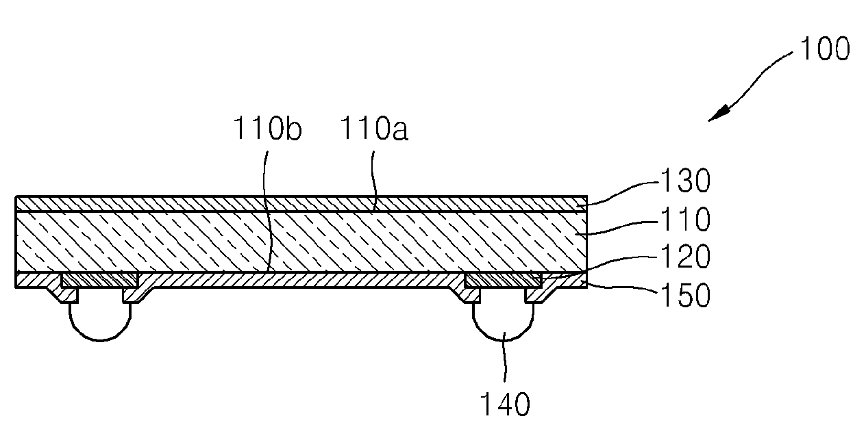
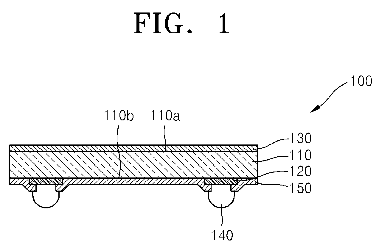
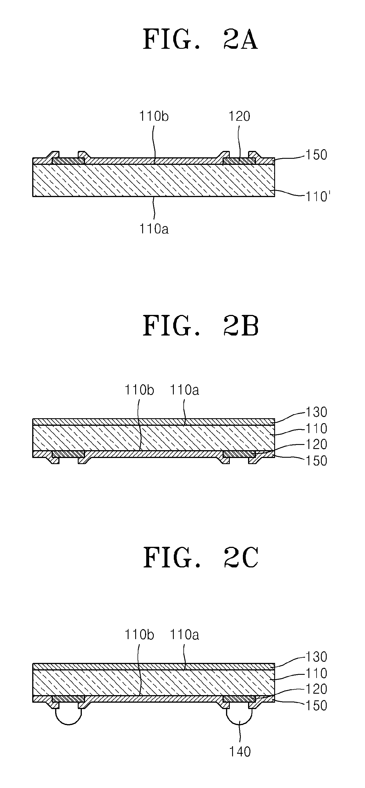
Semiconductor package
a technology of semiconductors and packages, applied in the field of semiconductor packages, can solve the problems of reduced device reliability and easy damage of thin semiconductor chips, and achieve the effects of reducing moisture absorption, superior semiconductor devices, and effectively blocking the penetration of metal ions
- Summary
- Abstract
- Description
- Claims
- Application Information
AI Technical Summary
Benefits of technology
Problems solved by technology
Method used
Image

Examples
experimental example 1
[0081]A semiconductor chip was formed on a semiconductor chip mounting unit which was formed of Cu and on which a nickel layer having a thickness of 4 μm was formed. An epoxy polymer resin layer including an amine group (—NH2) that was linked to a main chain was formed between the semiconductor chip mounting unit and the semiconductor chip. The epoxy polymer resin is commonly available and is obvious to one of ordinary skill in the art. Next, a resultant structure was sealed using EMC to form 96 CSPs.
[0082]An experiment was performed to check the occurrence of charge loss and delamination between the semiconductor chip and the semiconductor chip mounting unit of each of the semiconductor packages of the comparative example 1 and the experimental example 1, and results of the experiment are shown in Table 1. The experiment was performed by writing data to the semiconductor chips, leaving the semiconductor chips at a relative humidity of 85% and a temperature of 85oC for 24 hours, and...
PUM
 Abstract
Description
Claims
Application Information