Scan driving circuit and display device including the same

Inactive Publication Date: 2010-01-14
SONY CORP
View PDF12 Cites 21 Cited by
  • Summary
  • Abstract
  • Description
  • Claims
  • Application Information

AI Technical Summary

Benefits of technology

[0029]For a display device having the above-described display elements to operate, circuits have to be provided which supply signals to the scanning lines, initialization control lines, and display control lines. The circuits for supplying these signals are preferably circuits of an integrated structure, from the perspective of reduction in layout area

Problems solved by technology

Now, when configuring transistors of TFTs, irregularity in threshold voltage is unavoidable to a certain extent.
In the event that there is irregularity in the amount of current

Method used


Image

  • Scan driving circuit and display device including the same
  • Scan driving circuit and display device including the same
  • Scan driving circuit and display device including the same

Examples


Example

First Embodiment

[0126]The first embodiment relates to a scan driving circuit and to a display device having the scan driving circuit. The display device according to the first embodiment is a display device which uses display elements having a light emitting unit and a driving circuit thereof.

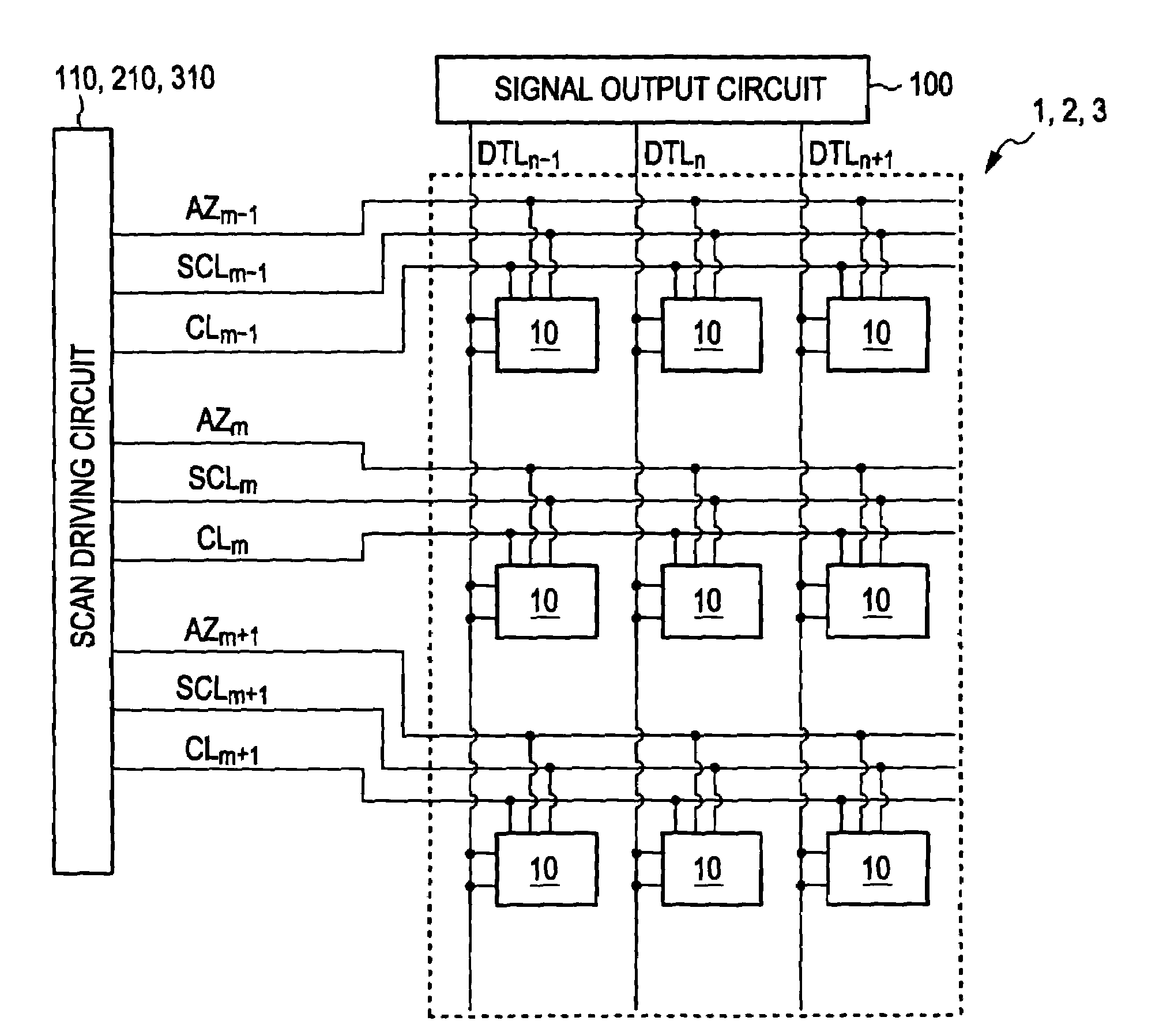
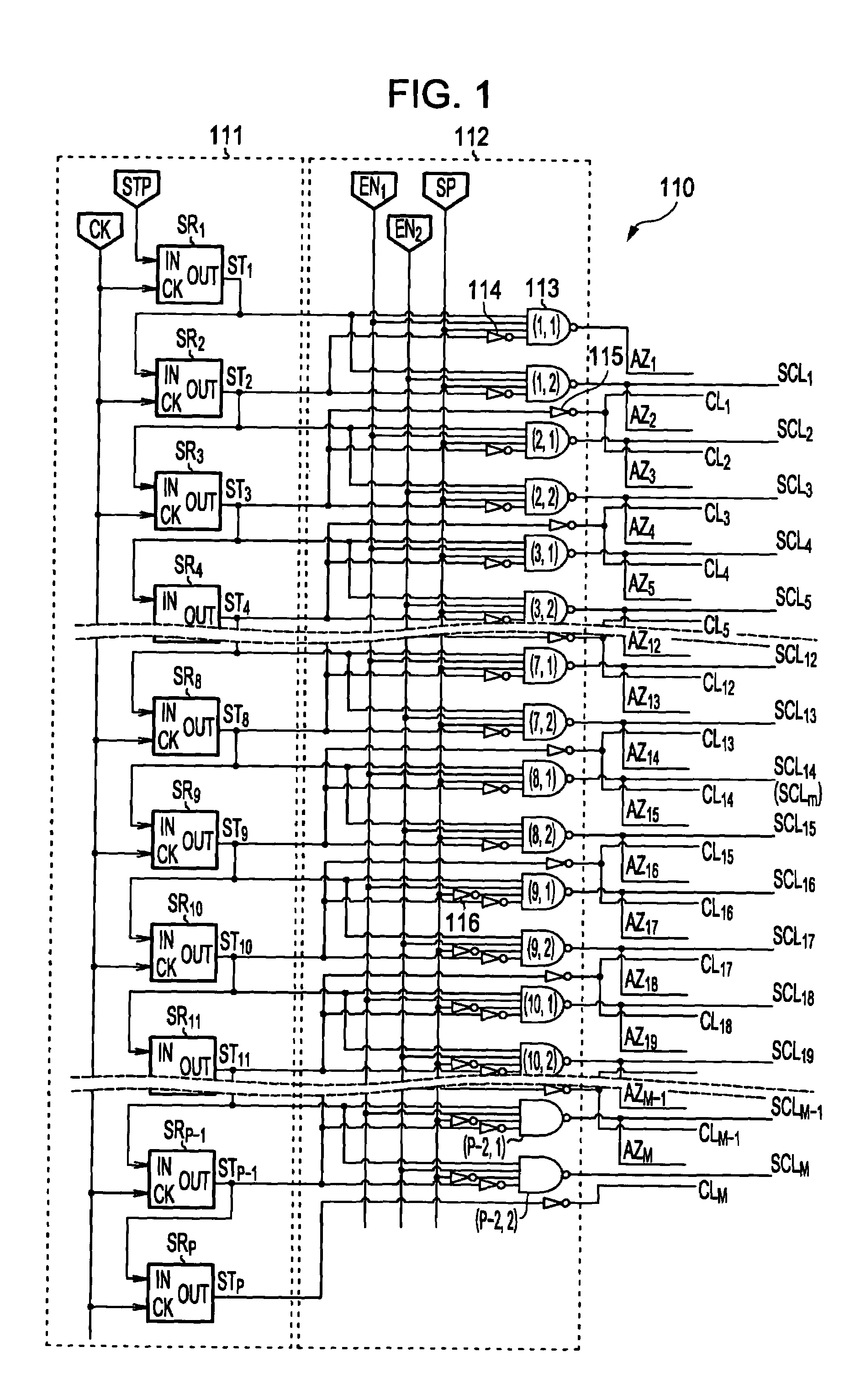
[0127]FIG. 1 is a circuit diagram of a scan driving circuit 110 according to the first embodiment, FIG. 2 is a conceptual diagram of a display device 1 according to the first embodiment, including the scan driving circuit shown in FIG. 1, FIG. 3 is a schematic timing chart of a shift register unit 111 configuring the scan driving circuit 110 shown in FIG. 1, FIG. 4 is a schematic timing chart of an upstream stage of a logic circuit unit 112 configuring the scan driving circuit 110 shown in FIG. 1, FIG. 5 is a schematic timing chart of a downstream stage of the logic circuit unit 112 making up the scan driving circuit 110 shown in FIG. 1, and FIG. 6 is an equivalent circuit diagram of a driving ...

Example

Second Embodiment

[0225]The second embodiment also relates to a scan driving circuit and to a display device having the scan driving circuit. As shown in FIG. 2, the display device 2 is of the same configuration as the display device 1 according to the first embodiment, other than the scan driving circuit being different. Accordingly, description of the display device 2 according to the second embodiment will be omitted.

[0226]FIG. 16 is a circuit diagram of a scan driving circuit according to a second embodiment, FIG. 17 is a schematic timing chart of a shift register unit making up the scan driving circuit shown in FIG. 16, FIG. 18 is a schematic timing chart of an upstream stage of a logic circuit unit 212 making up the scan driving circuit 210 shown in FIG. 16, and FIG. 19 is a schematic timing chart of a downstream stage of a logic circuit unit 212 making up the scan driving circuit 210 shown in FIG. 16.

[0227]With the scan driving circuit 110 according to the first embodiment, th...

Example

Third Embodiment

[0251]The third embodiment also relates to a scan driving circuit and to a display device having the scan driving circuit. As shown in FIG. 2, the display device 3 according to the third embodiment is of the same configuration as the display device 1 according to the first embodiment, other than the scan driving circuit being different. Accordingly, description of the display device 3 according to the third embodiment will be omitted.

[0252]FIG. 21 is a circuit diagram of a scan driving circuit 310 according to the third embodiment, FIG. 22 is a schematic timing chart of a shift register unit 311 making up the scan driving circuit 310 shown in FIG. 21, FIG. 23 is a schematic timing chart of an upstream stage of a logic circuit unit 312 making up the scan driving circuit 310 shown in FIG. 21, and FIG. 24 is a schematic timing chart of a downstream stage of the logic circuit unit 312 making up the scan driving circuit 310 shown in FIG. 21.

[0253]With the scan driving cir...


PUM


Abstract

A scan driving circuit includes a shift register unit and a logic circuit unit. The start of a start pulse of an output signal STp+1 of a p+1'th shift register is situated between the start and end of a start pulse of the output signal STp of a p'th shift register, and one each of a first enable signal through a Q'th enable signal exist in sequence between the start of the start pulse of the output signal STp and the start of the start pulse of the output signal STp+1. The operations of a (p′, q)'th NAND circuit are restricted based on period identifying signals, such that the NAND circuit generates scanning signals based only on a portion of the output signal STP corresponding to the first start pulse, the signal obtained by inverting the output signal STp+1, and the q'th enable signal ENq.

Description

BACKGROUND OF THE INVENTION[0001]1. Field of the Invention[0002]The present invention relates to a scan driving circuit and to a display device including the scan driving circuit. More particularly, the present invention relates to a scan driving circuit and to a display device including the scan driving circuit, in which signals can be supplied to scanning lines, initialization control lines, and display control lines, and a lit / unlit state of display elements can be switched multiple times during one field period by supplying multiple pulse signals to the display control lines during the field period, without affecting the signals being supplied to the scanning lines and initialization control lines.[0003]2. Description of the Related Art[0004]Examples of widely used display devices having display elements arranged in the form of a two-dimensional matrix include liquid crystal display devices made up of liquid crystal cells driven by voltage, and also display devices including lig...

Claims


Application Information

Patent Timeline
IPC IPC(8): G06F3/038G09G3/30
CPCG09G3/3233G09G3/3266G09G2300/0819G09G2300/0842G09G3/30G09G2310/0286G09G3/3291G09G3/3258G09G2300/0861G09G2230/00G09G2300/0426G09G3/20G09G3/32G09G2300/0814G09G2300/0871G09G2300/0443G09G2300/0452
Inventor TANIKAME, TAKAOJINTA, SEIICHIRO
Owner SONY CORP
Why Eureka
Try Eureka