Junction Field Effect Transistor Using Silicide Connection Regions and Method of Fabrication

a junction field effect and connection region technology, applied in the direction of transistors, semiconductor devices, electrical equipment, etc., can solve the problems of reducing the efficiency of transistors, and achieve the effect of reducing contact resistance and improving the operation of semiconductor devices

Inactive Publication Date: 2010-01-28
DSM SOLUTIONS
View PDF5 Cites 0 Cited by
  • Summary
  • Abstract
  • Description
  • Claims
  • Application Information

AI Technical Summary

Benefits of technology

[0008]The contact resistance at an interface between silicide and silicon is lower than the contact resistance at the interface between polysilicon and silicon. In particular, the contact resistance at an interface between polysilicon and silicon is approximately 200 Ω·μm2, whereas the contact resistance at an interface between silicide and silicon, is approximately 10 Ω·μm2. Thus, for a given area of contact, the contact resistance at an interface between a first connection region and a source region, and between a second connection region and a drain region, is reduced when those first and second connection regions are formed using silicide rather than polysilicon. By reducing the contact resistance at these interfaces in this way, the operation of semiconductor device is improved.

Problems solved by technology

The voltage drop that results from this contact resistance reduces the efficiency of the transistor.

Method used


Image

  • Junction Field Effect Transistor Using Silicide Connection Regions and Method of Fabrication
  • Junction Field Effect Transistor Using Silicide Connection Regions and Method of Fabrication
  • Junction Field Effect Transistor Using Silicide Connection Regions and Method of Fabrication

Examples


Embodiment Construction

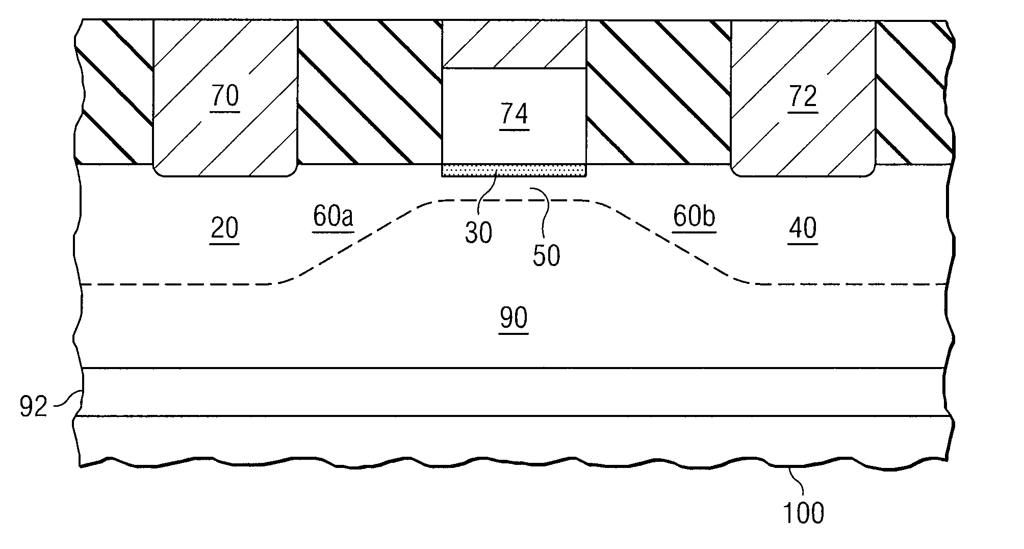
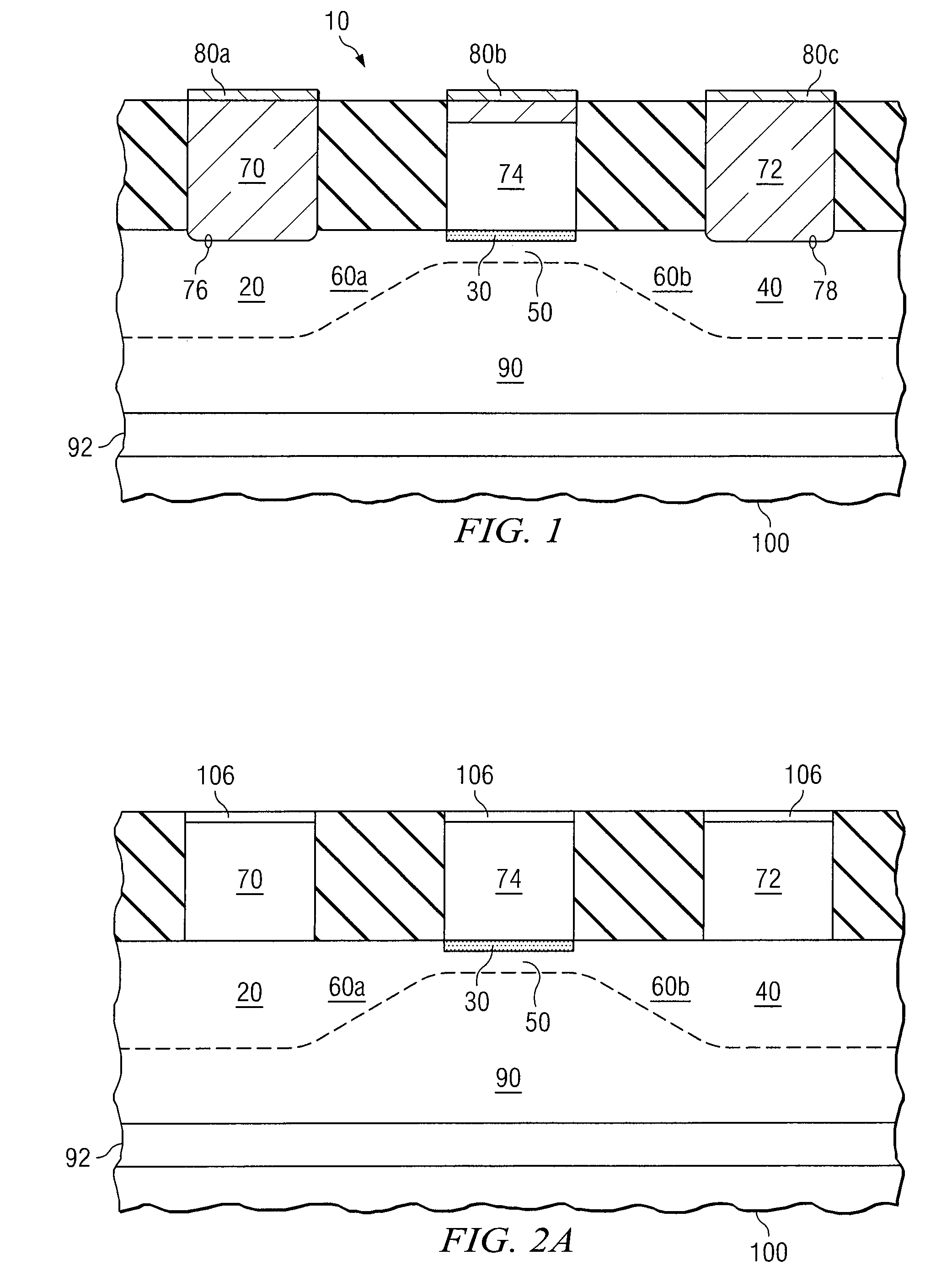
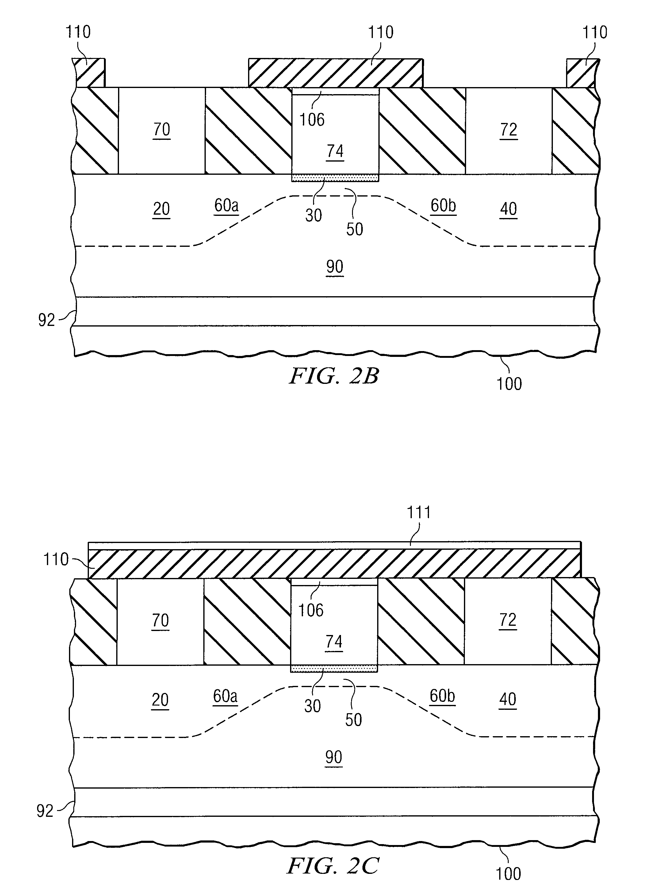
[0013]FIG. 1 illustrates a semiconductor device 10, according to certain embodiments. As shown in FIG. 1, device 10 may comprise a source region 20, a gate region 30, a drain region 40, a channel region 50, link regions 60a-b, silicide connection regions 70 and 72, polysilicon connection region 74, well region 90, and substrate 100. In some embodiments of device 10 using a Silicon-On-Insulator (SOI) architecture, device 10 further includes an insulating layer 92 between well region 90 and substrate 100. These regions are not necessarily drawn to scale. An interface 76 exists between silicide connection region 70 and source region 20. An interface 78 exists between silicide connection region 72 and drain region 40. In some embodiments, semiconductor device 10 is a junction field effect transistor (JFET). When appropriate voltages are applied to connection regions 70, 72, and 74 of semiconductor device 10, a current flows through channel region 50 between source region 20 and drain re...


PUM


Abstract

A junction field effect transistor comprises a semiconductor substrate and a well region formed in the substrate. A source region of a first conductivity type is formed in the well region. A drain region of the first conductivity type is formed in the well region and spaced apart from the source region. A channel region of the first conductivity type is located between the source region and the drain region and formed in the well region. A gate region of a second conductivity type is formed in the well region. The transistor further includes first, second, and third connection regions. The first connection region is in ohmic contact with the source region and formed of silicide. The second connection region is in ohmic contact with the drain region and formed of silicide. The third connection region in ohmic contact with the gate region.

Description

TECHNICAL FIELD OF THE INVENTION[0001]The present disclosure relates generally to semiconductor devices and more particularly to a junction field effect transistor using silicide connection regions.BACKGROUND OF THE INVENTION[0002]In current transistor technologies, the contact terminals are formed using a polysilicon material while the active regions are formed using silicon. The current that flows from one contact terminal, such as a source terminal, to another contact terminal, such as a drain terminal, faces a contact resistance at the interface between the polysilicon and silicon materials. The voltage drop that results from this contact resistance reduces the efficiency of the transistor.SUMMARY OF THE INVENTION[0003]In accordance with the present invention, the disadvantages and problems associated with prior junction field effect transistors using polysilicon contact terminals have been substantially reduced or eliminated.[0004]In accordance with one embodiment of the presen...

Claims


Application Information

Patent Timeline
Patent Type & Authority Applications(United States)
IPC IPC(8): H01L29/80H01L21/337
CPCH01L29/458H01L29/8086H01L29/66901
Inventor KAPOOR, ASHOK K.VORA, MADHUKAR B
Owner DSM SOLUTIONS
Why Eureka
Try Eureka