

Method of manufacturing printed circuit board
a printed circuit board and manufacturing method technology, applied in the direction of metallic material coating process, synthetic resin layered products, pretreated surfaces, etc., can solve the problems of difficult realization of fine circuits with less than 50 m pitch (l/s=25/25 m), difficult to generate heat, etc., and achieve high-reliability fine circuits
Inactive Publication Date: 2010-01-28
SAMSUNG ELECTRO MECHANICS CO LTD
View PDF7 Cites 2 Cited by
- Summary
- Abstract
- Description
- Claims
- Application Information
AI Technical Summary
Benefits of technology
[0021]Accordingly, an object of the present invention is to provide a PCB, in which interfacial adhesion of a resin substrate is increased without changing the surface roughness thereof, thus forming a highly reliable fine circuit, and also a method of manufacturing such a PCB.
[0023]A further object of the present invention is to provide a PCB, which may be manufactured in an environmentally friendly manner by replacing a typical wet copper plating process with a dry copper plating process, and also a method of manufacturing such a PCB.
Problems solved by technology
As such, although the material for the resin insulating layer is typically exemplified by epoxy resin, such as FR-4, BT (Bismaleimide Triazine), or ABF (Ajinomoto Build up Film), it is disadvantageous because it has a high dielectric constant (Dk>3.5-[ABF]˜4.5[BT, FR-4]) and a high loss coefficient (Df>0.05), and undesired signal transfer rate and transfer loss are caused, consequently generating heat and deteriorating electrical properties.
Ultimately, a fine circuit having a pitch of less than 50 μm (L / S=25 / 25 μm) is difficult to realize.
However, due to the use of expensive ABF material, the process cost is increased, leading to a high production price.
Furthermore, a fine circuit is difficult to realize, attributable to wet surface treatment and electroless chemical plating.
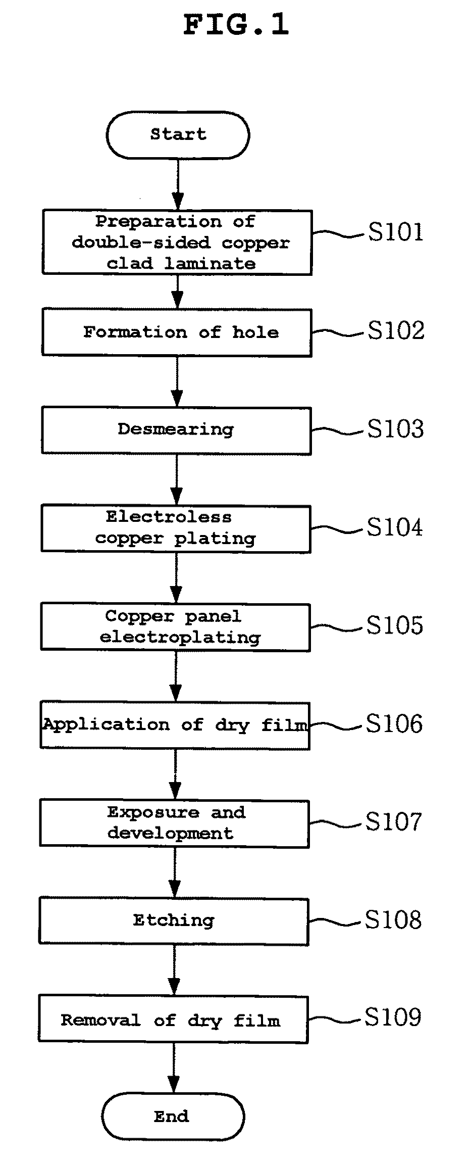
However, in the conventional SAP, since the copper layer is formed through a wet process such as wet surface treatment and electroless plating, the surface roughness is enlarged, and the formation of the fine circuit is limited.
As well, a lot of waste is generated, therefore the above process is considered environmentally unfriendly.
Method used
View moreImage
Smart ImageViewing Examples

Examples
example 1
[0081]Both surfaces of a polyimide resin substrate, used as a base material, were coated several times with PTFE under conditions of a temperature of 350˜420° C. and humidity of
[0082]The peel strength and surface roughness of the PCB thus manufactured were measured. The results are shown in Table 2 below.
example 2
[0083]Both surfaces of a polyimide resin substrate, used as a base material, were coated several times with TPI under conditions of a temperature of 250˜350° C. and humidity of
[0084]The peel strength and surface roughness of the PCB thus manufactured were measured. The results are shown in Table 2 below.
Login to View More PUM
| Property | Measurement | Unit |
|---|---|---|
| surface roughness | aaaaa | aaaaa |
| surface roughness | aaaaa | aaaaa |
| surface roughness | aaaaa | aaaaa |
Abstract
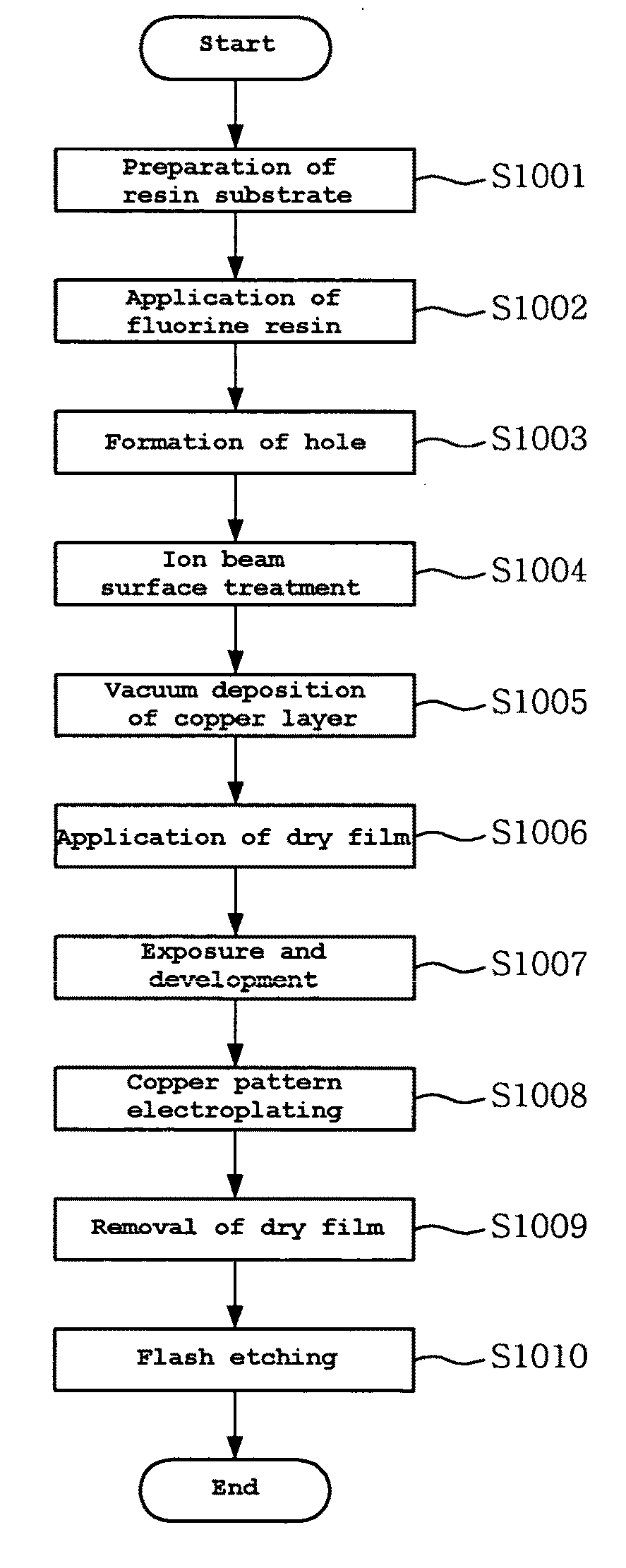
A method of manufacturing the same, in which a fluorine resin coating layer is formed on a resin substrate, and then a copper layer is formed using a dry process including ion beam surface treatment and vacuum deposition instead of a conventional wet process including surface roughening and electroless copper plating. The interfacial adhesion of the substrate material may be increased without changing the surface roughness thereof, thus realizing a highly reliable fine circuit. As well, a low dielectric constant and a low loss coefficient may be obtained thanks to the formation of the fluorine resin layer. Further, a wet process is replaced with a dry process, whereby the copper plating layer may be formed in an environmentally friendly manner.
Description
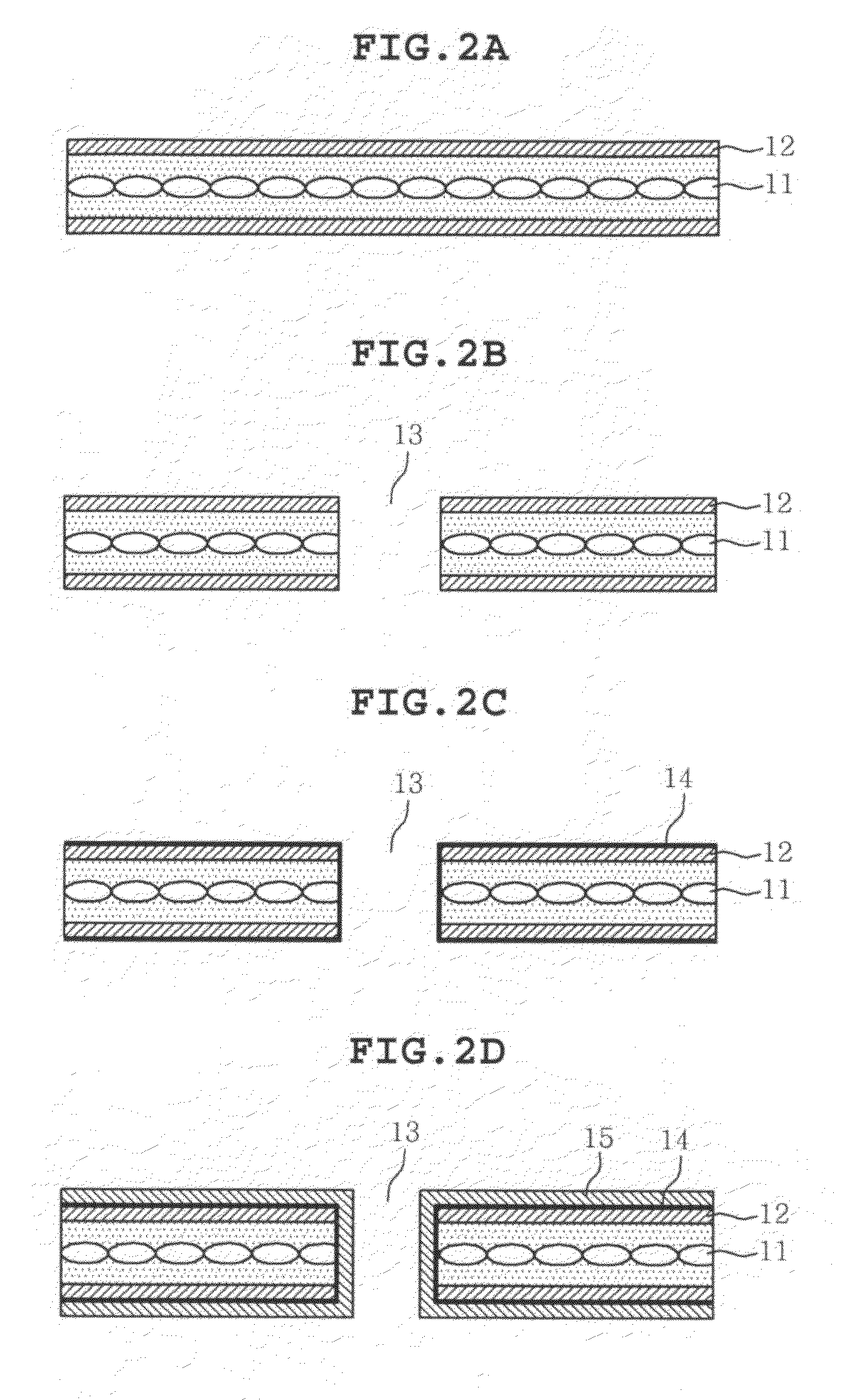
CROSS-REFERENCE TO RELATED APPLICATIONS[0001]This application is a U.S. divisional application filed under 35 USC 1.53(b) claiming priority benefit of U.S. Ser. No. 11 / 585,276 filed in the United States on Oct. 24, 2006, which claims earlier priority benefit to Korean Patent Application No. 10-2005-0125249 filed with the Korean Intellectual Property Office on Dec. 19, 2005, and Korean Patent Application No. 10-2006-0063370 filed with the Korean Intellectual Property Office on Jul. 6, 2006, the disclosures of which are incorporated herein by reference.BACKGROUND OF THE INVENTION[0002]1. Field of the Invention[0003]The present invention relates to a printed circuit board (PCB) and a method of manufacturing the same. More particularly, the present invention relates to a PCB, in which a hydrophilic fluorine resin coating layer is formed on a resin substrate and a dry plating process is performed instead of a conventional wet plating process, thus obtaining a highly reliable fine circuit...
Claims
Login to View More Application Information
Patent Timeline
 Patent Type & AuthorityApplications(United States)
IPC IPC(8): B05D3/06C23C14/34C08J7/043C08J7/056
CPCB32B3/266Y10T428/24917B32B27/28C08J7/045H05K1/034H05K1/036H05K3/108H05K3/381H05K3/426H05K2201/015H05K2203/092B32B27/16B32B27/281B32B27/304B32B27/322B32B27/38B32B2255/10B32B2255/205B32B2255/26B32B2255/28B32B2307/728B32B2457/08B32B27/08C08J7/0423C08J7/043C08J7/056
InventorSONG, JONG SEOKKIM, TAEHOON
OwnerSAMSUNG ELECTRO MECHANICS CO LTD