

Method and apparatus for multi-die thermal analysis
a multi-die integrated circuit and thermal analysis technology, applied in the field of multi-die thermal analysis, can solve the problems of electrical damage, physical damage to the components (e.g., circuits) of the ic, and the amount of leakage current, and achieve the effect of facilitating the solving of the overall heat flow equation
- Summary
- Abstract
- Description
- Claims
- Application Information
AI Technical Summary
Benefits of technology
Problems solved by technology
Method used
Image

Examples
Embodiment Construction
[0034]In the following description, numerous details are set forth for the purpose of explanation. However, one of ordinary skill in the art will realize that the invention may be practiced without the use of these specific details. In other instances, well-known structures and devices are shown in block diagram form in order not to obscure the description of the invention with unnecessary detail.
I. Overview
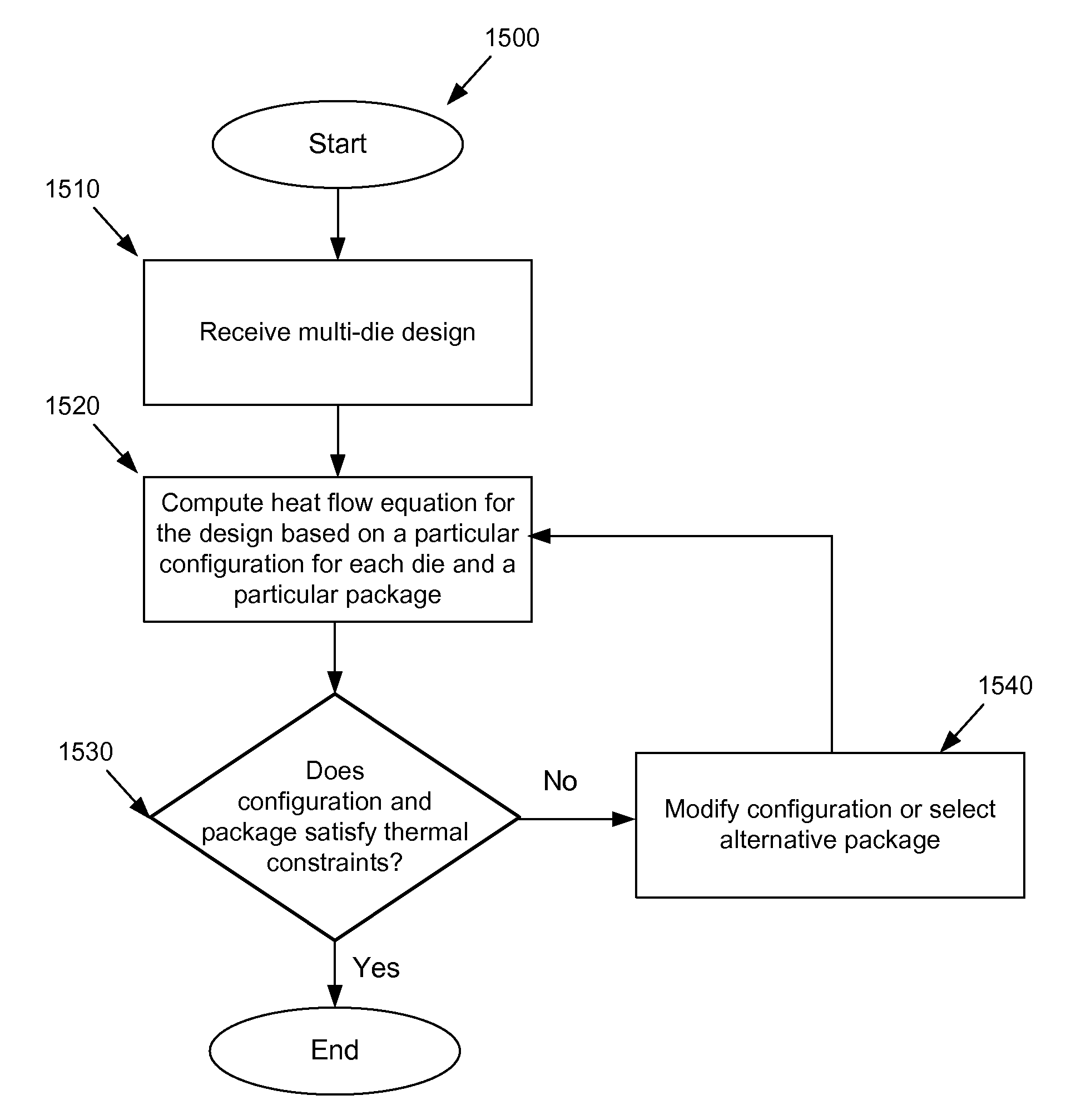
[0035]Some embodiments of the invention provide a method for performing thermal analysis of a multi-die integrated circuit (IC) design layout. The thermal analysis produces a temperature distribution for analyzing internal properties of each die within the multi-die design and for analyzing thermal interactions between two or more dies of the design based on an internal configuration of the two or more dies. Therefore, in some embodiments, the temperature distribution shows a temperature distribution for each die and the individual temperature distributions show varying temperatu...
PUM
 Abstract
Description
Claims
Application Information