Edge detection method
- Summary
- Abstract
- Description
- Claims
- Application Information
AI Technical Summary
Benefits of technology
Problems solved by technology
Method used
Image
Examples
first embodiment
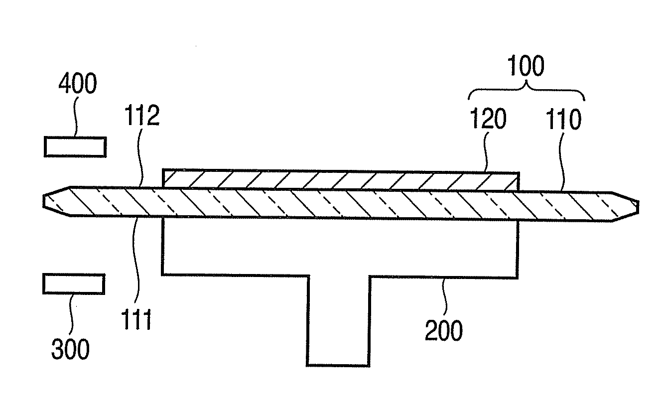
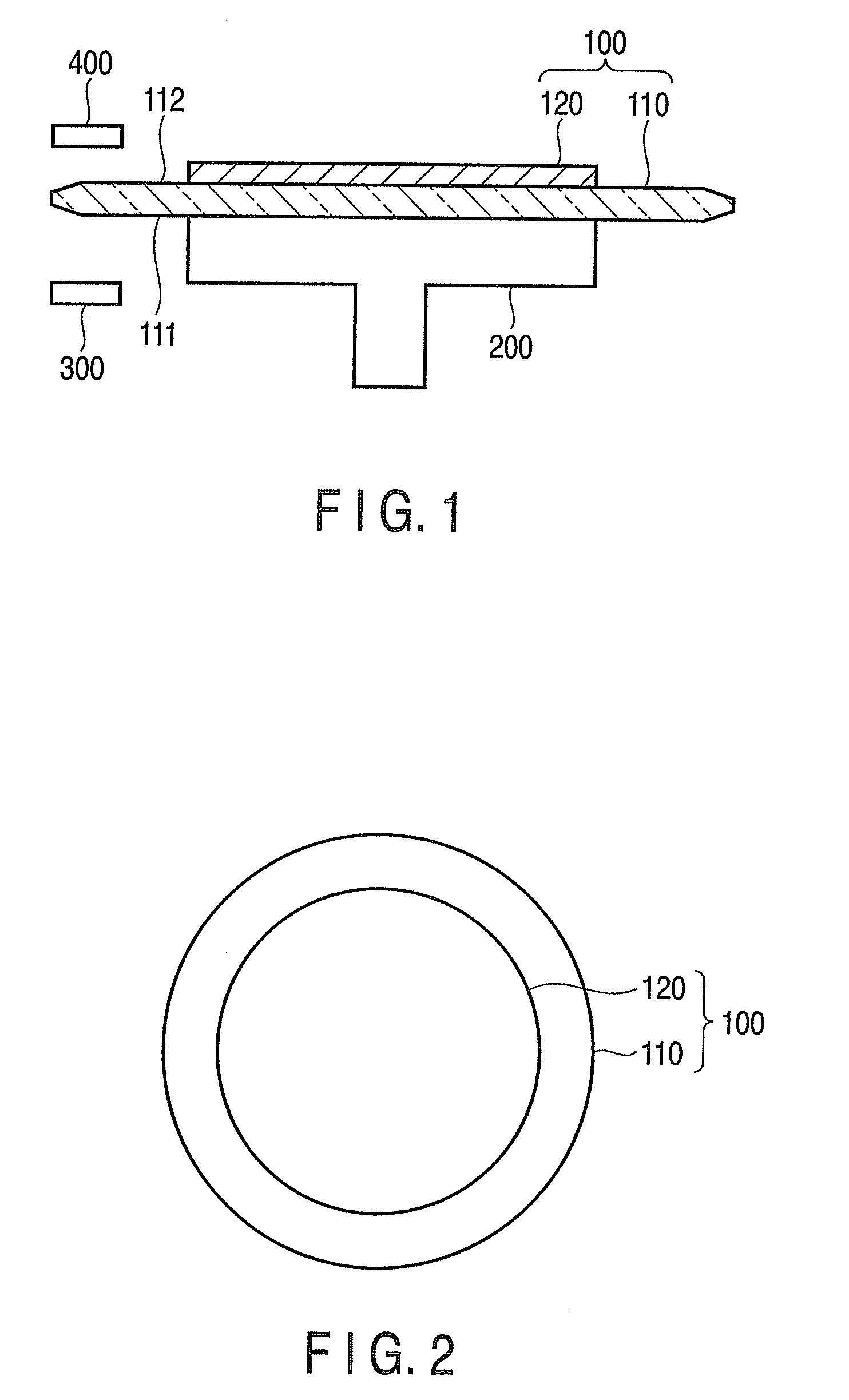
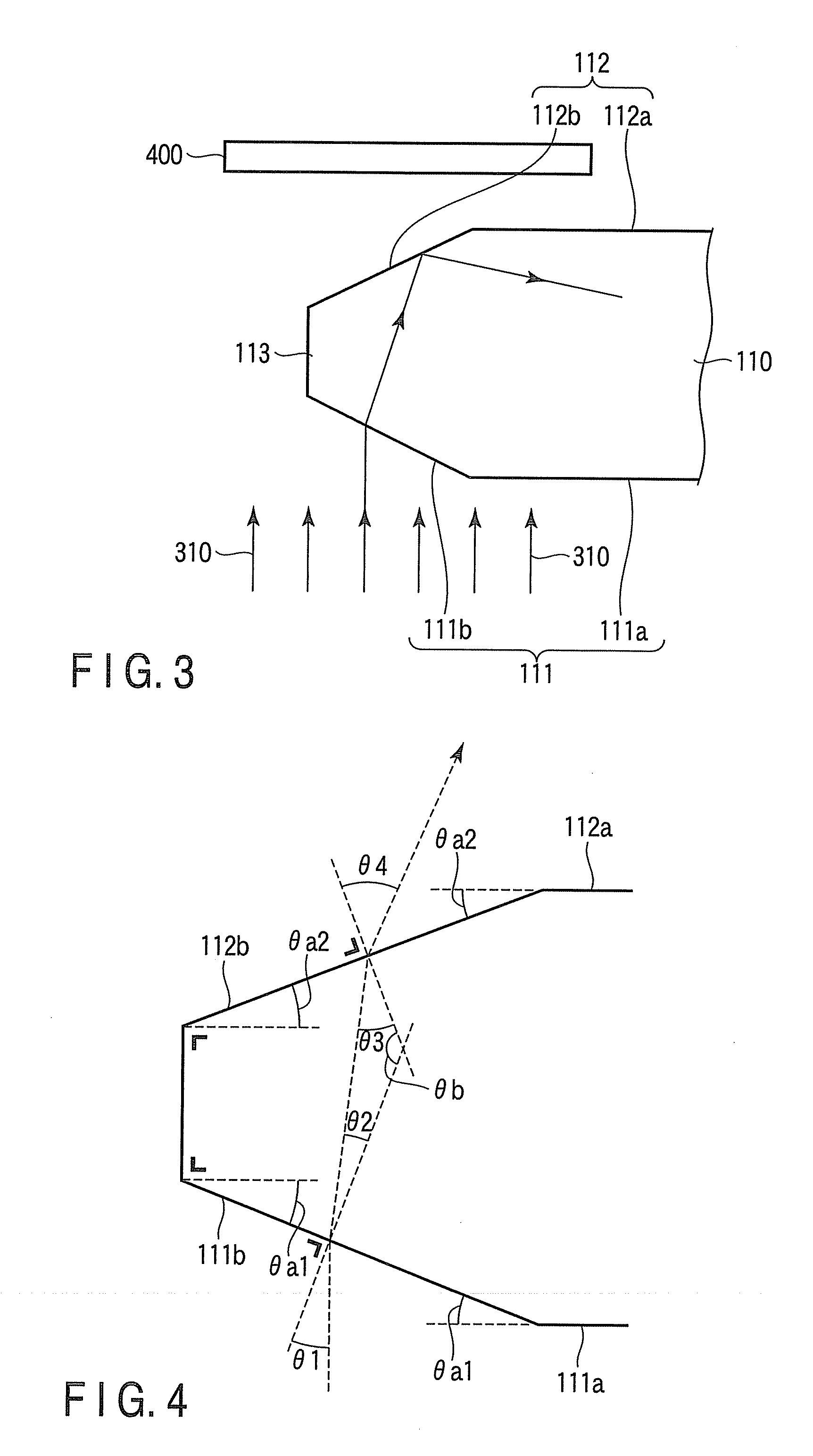
[0020]FIG. 1 is a schematic view to explain an edge detection method according to a first embodiment of the invention. FIG. 2 is a schematic plan view showing the configuration of a substrate to be processed shown in FIG. 1. FIG. 3 is a detail view of a part of FIG. 1.
[0021]A substrate to be processed 100 is composed of a transparent substrate 110, such as a glass substrate, and a semiconductor substrate (or a semiconductor wafer) 120 provided on the transparent substrate 110. On the semiconductor substrate 120, an element region including active elements and interconnections is provided. In the first embodiment, an image sensor (e.g., a CMOS image sensor) including light-receiving elements and transistors is formed in the element region. The transparent substrate 110 is for securing the mechanical strength of the semiconductor substrate 120 and protecting the element region of the semiconductor substrate 120. The substrate 100 is placed on a stage 200 and can be rotated by the rota...
second embodiment
[0048]Next, an edge detection method according to a second embodiment of the invention will be explained. Since the basic configuration and method are the same as those of the first embodiment, what has been explained in the first embodiment will be omitted.
[0049]FIG. 8 is a detail view of a part of FIG. 1. Hereinafter, referring to FIG. 8, the principle of edge detection in the second embodiment will be explained.
[0050]As shown in FIG. 8, a transparent substrate 110 has a first main face 111 and a second main face 112. The first main face 111 has a first main region 111a and a first peripheral region 111b outside the first main region 111a. The second main face 112 has a second main region 112a in parallel with the first main region 111a and a second peripheral region 112b outside the second main region 112a. The inclination of the first peripheral region 111b and that of the second peripheral region 112b become gentler toward the center of the transparent substrate 110. That is, t...
PUM
 Abstract
Description
Claims
Application Information


