
Organic luminescent device and method for manufacturing the same

a luminescent device and organic technology, applied in the field of luminescent devices, can solve the problems of increasing the difficulty of manufacturing such luminescent devices by using the conventional shadow mask, defective light emission of luminescent devices, and various problems, so as to improve the aperture ratio, reduce the size, and prevent defective light emission

Active Publication Date: 2013-11-05
CANON KK
View PDF2 Cites 0 Cited by
  • Summary
  • Abstract
  • Description
  • Claims
  • Application Information

AI Technical Summary

Benefits of technology

[0010]A disclosed aspect of the embodiments is directed to allowing a luminescent device including luminescent layers patterned by photolithography to prevent exhibiting defective light emission or undergoing a voltage increase attributable to, for example, disconnection or resistance increase of the second electrode, while utilizing advantages of photolithography such as reduction in the pixel size and improvement in the aperture ratio.
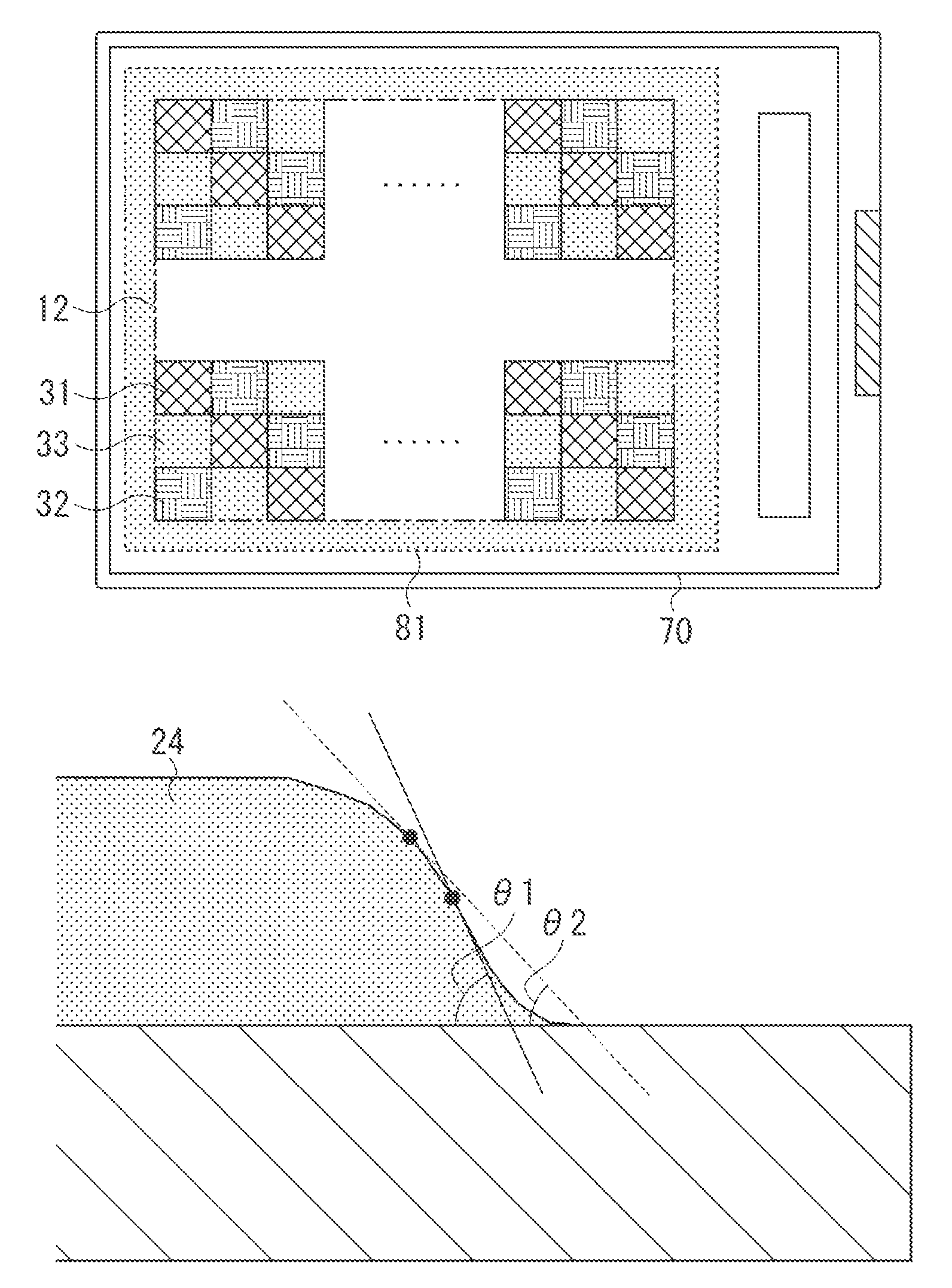
[0012]The luminescent device according to one embodiment includes luminescent layers patterned by photolithography, and an end portion of an organic compound layer that is not located between organic EL elements is formed to have a smaller inclination angle in the inclined area with respect to the substrate (herein after referred to as inclination angle). Thus, while utilizing advantages of photolithography such as reduction of the size and improvement of the aperture ratio, one embodiment may prevent defective light emission or a voltage increase attributable to disconnection or resistance increase of the second electrode caused in the inclined area outside the element area.

Problems solved by technology

Meanwhile, high-definition luminescent devices exceeding 300 pixels per inch (ppi) has been recently demanded, and it is becoming increasingly difficult to manufacture such luminescent devices by using the conventional shadow mask.
Consequently, various problems are caused.
In other cases, the luminescent device exhibits defective light emission such as shading or undergoes a voltage increase.

Method used


Image

  • Organic luminescent device and method for manufacturing the same
  • Organic luminescent device and method for manufacturing the same
  • Organic luminescent device and method for manufacturing the same

Examples


Embodiment Construction

[0020]Various exemplary embodiments, features, and aspects of the embodiments will be described in detail below with reference to the drawings.

[0021]Conventional techniques in the relevant technical field may be applied to what is not particularly illustrated or described in this specification. In addition, while the disclosure will be hereinafter described based on the following exemplary embodiments, the disclosure is not limited thereto. Various modifications may suitably be made within the technical scope of the embodiments.

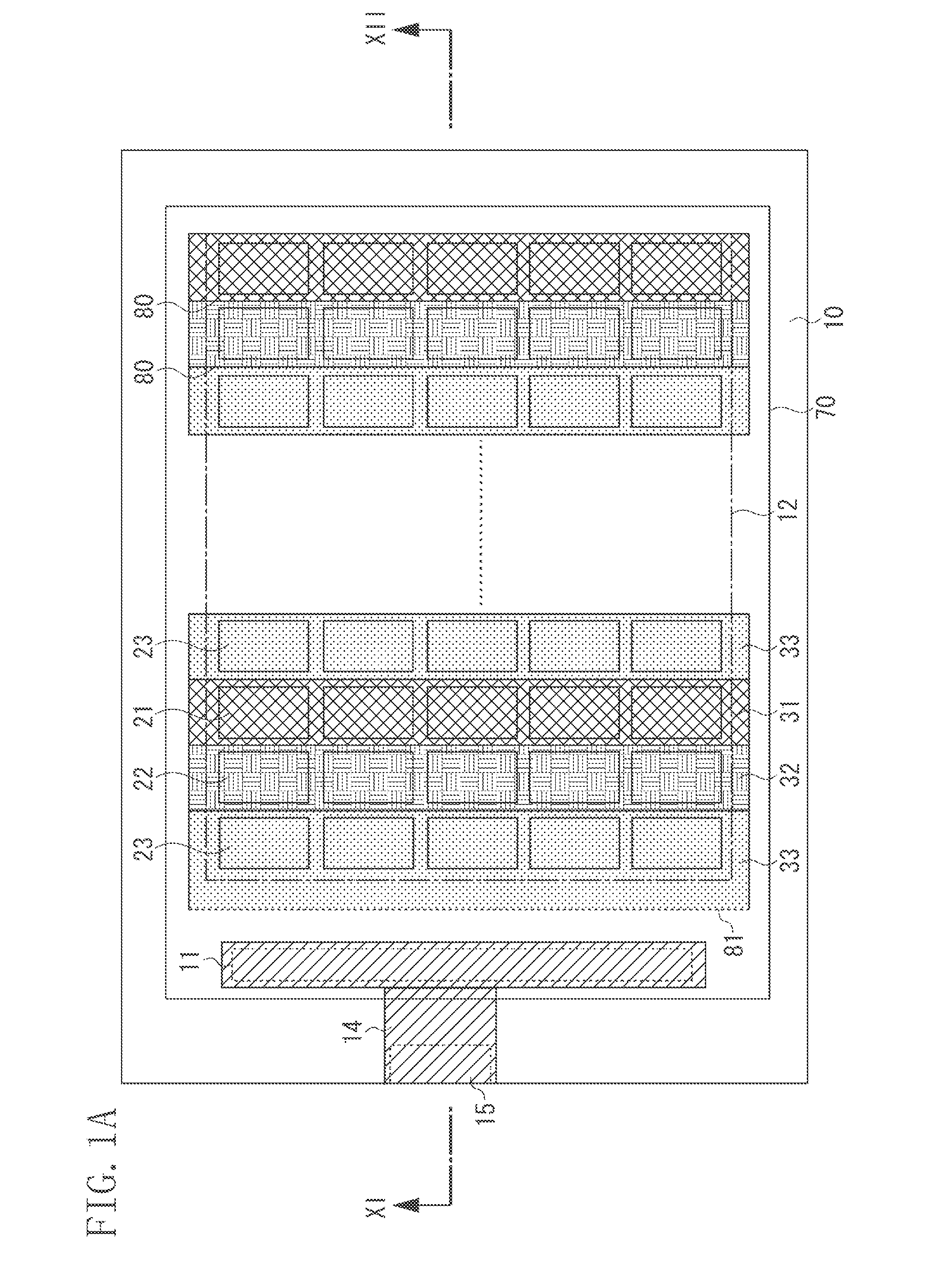
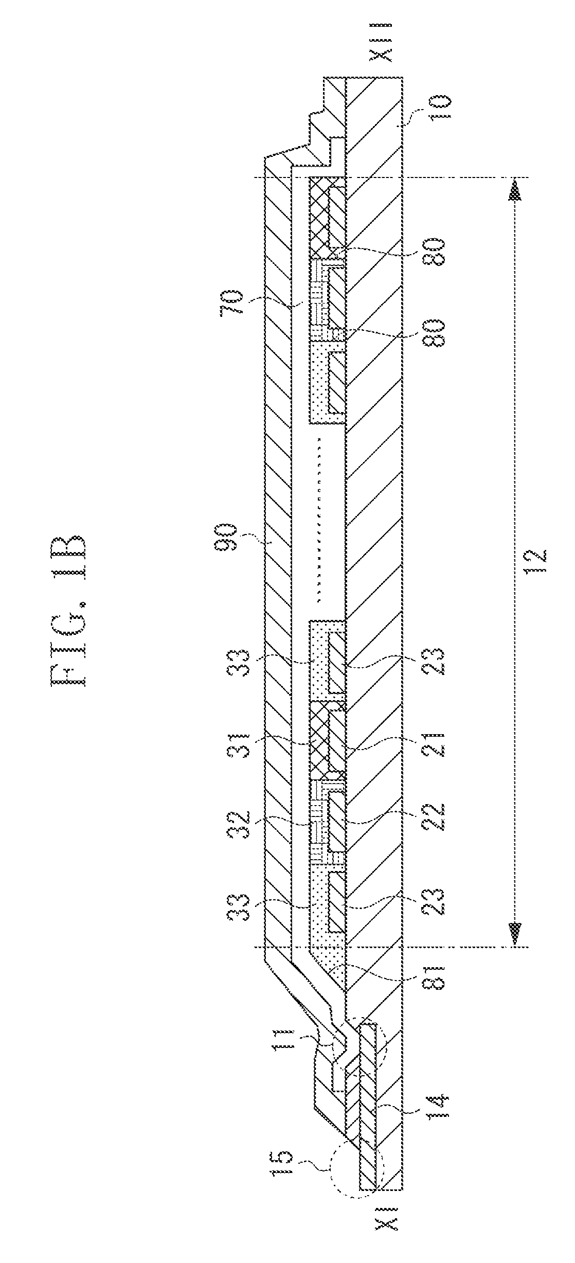
[0022]FIG. 1A is a schematic plan view illustrating a luminescent device, and FIG. 1B is a schematic cross section illustrating the luminescent device taken along line XI-XII in FIG. 1A. An external connection terminal 15 and a wiring 14 that is electrically connected to the external connection terminal 15 are formed outside an element area 12 of a substrate 10. Organic EL elements are formed in the element area 12. The substrate 10 includes a supporting memb...


PUM


Abstract

Among end portions of a plurality of organic compound layers patterned by photolithography, an end portion in an area that is not located between luminescent elements and that is located in an area covered with a second electrode is formed to have a smaller inclination angle than that of an end portion located between the luminescent elements.

Description

BACKGROUND OF THE INVENTION[0001]1. Field of the Invention[0002]One disclosed aspect of the embodiments relates to a luminescent device capable of displaying at least two different colors, and particularly to an organic electroluminescent (EL) device including at least a first EL element and a second organic EL element, each of which emits light of a different color.[0003]2. Description of the Related Art[0004]In a method for manufacturing an organic EL device capable of displaying a plurality of colors, a shadow mask is widely used to selectively form a luminescent layer that emits a specific color in a specific area. Meanwhile, high-definition luminescent devices exceeding 300 pixels per inch (ppi) has been recently demanded, and it is becoming increasingly difficult to manufacture such luminescent devices by using the conventional shadow mask. Japanese Patent No. 4578026 discusses, as a technique capable of miniaturization, a method in which luminescent layers are selectively for...

Claims


Application Information

Patent Timeline
Patent Type & Authority Patents(United States)
IPC IPC(8): H01J1/62
CPCH01L51/5012H01L51/5209H01L51/5225H01L27/3211H10K59/35H10K71/233H10K50/813H10K50/822H10K50/11H10K71/166
Inventor KIMURA, TOSHIHIDEHIROKI, TOMOYUKIOTSUKA, MANABUSATO, NOBUHIKO
Owner CANON KK
Learn More