Metal material and its manufacturing method, thin-film device and its manufacturing method, element-side substrate and its manufacturing method, and liquid crystal display and its manufacturing method

a technology of metal materials and manufacturing methods, applied in the direction of optical elements, instruments, transportation and packaging, etc., can solve the problems of deteriorating the optical performance of the liquid crystal display apparatus, increasing the number of manufacturing steps, etc., to prevent an electrical corrosion, eliminate or reduce the difference of work functions, and excellent image quality

Inactive Publication Date: 2010-02-11
SHARP KK
View PDF5 Cites 8 Cited by
  • Summary
  • Abstract
  • Description
  • Claims
  • Application Information

AI Technical Summary

Benefits of technology

[0053]When the metal material and a thin-film device using the metal material according to the present invention are applied to the semi-transmissive reflective liquid crystal display apparatus, the work function of the uppermost layer of the reflective electrode is controlled by a plasma treatment so as to be within a difference of ±0.2 eV with respect to the work function of the transmissive electrode. Thus, the difference between the optimum direct current offset voltage for the reflective electrode and the optimum direct current offset voltage for the transmissive electrode is reduced, thereby obtaining an excellent image quality. The reflective electrode and the transparent electrode each can be a single layer film or can be a laminated layer film.
[0054]Aluminum (Al) or a material including aluminum (aluminum alloy or the like) can be used for the reflective electrode or the uppermost layer of the reflective electrode, the work function of which is controlled by the plasma treatment. When the reflective electrode is a laminated layer film, it is possible, by forming a metal layer with a high melting temperature made of, such as molibudenum (Mo), as a lower layer, to prevent an electrical corrosion in an Al film and an ITO film due to resist developing solution, etching solution or the like. The plasma treatment can be performed using a fluorine-based gas, such as CF4.
[0055]As described above, according to the present invention, by performing a plasma treatment on a metal material, it is possible to control the work function of the metal material by changing at least a predetermined value (a range within 0.1 eV or more and 0.6 eV or less, or a range within 0.1 eV or more and 1.0 eV or less). This allows the elimination or the reduction in the difference of the work functions in different metal thin films in a thin-film device. When this is applied to the semi-transmissive reflective liquid crystal display apparatus, the difference of the work functions in a reflective electrode and a transparent electrode can be eliminated or reduced. As a result, the difference between the optimum direct current offset voltage for the reflective electrode and the optimum direct current offset voltage for the transmissive electrode is eliminated or reduced, thereby manufacturing a liquid crystal display apparatus having an excellent image quality with no display flicker. Further, since no unnecessary film is laminated on the reflective electrode as is in the conventional techniques, the problem of increasing the number of the manufacturing steps and deteriorating the optical performance of the liquid crystal display apparatus does not occur.

Problems solved by technology

Therefore, a problem of increasing the number of the manufacturing steps occurs.
In addition, since a film is laminated on the reflective electrode, a problem of deteriorating the optical performance of the liquid crystal display apparatus occurs.

Method used


Image

  • Metal material and its manufacturing method, thin-film device and its manufacturing method, element-side substrate and its manufacturing method, and liquid crystal display and its manufacturing method
  • Metal material and its manufacturing method, thin-film device and its manufacturing method, element-side substrate and its manufacturing method, and liquid crystal display and its manufacturing method
  • Metal material and its manufacturing method, thin-film device and its manufacturing method, element-side substrate and its manufacturing method, and liquid crystal display and its manufacturing method

Examples


Embodiment Construction

[0091]Hereinafter, a case will be described in detail with reference to the accompanying drawings, in which an embodiment of a metal material according to the present invention having the work function thereof controlled by changing by at least a predetermined value by a plasma treatment and a method for manufacturing the metal material; and a thin-film device using the metal material for a metal thin film material and a method for manufacturing the thin-film device is applied to an element-side substrate, a semi-transmissive reflective liquid crystal display apparatus using a method for manufacturing the element-side substrate, and a method for the semi-transmissive reflective liquid crystal display apparatus.

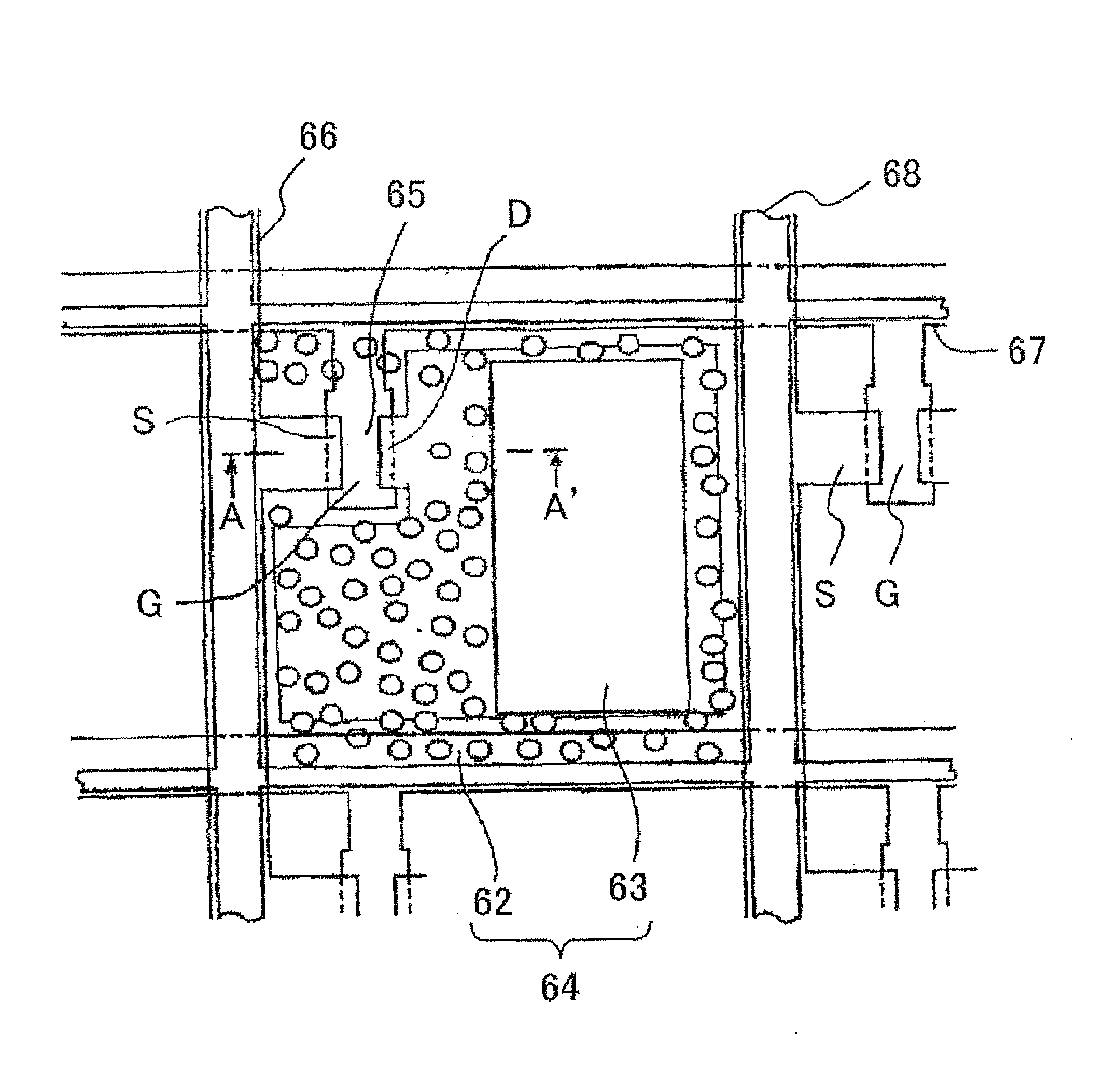
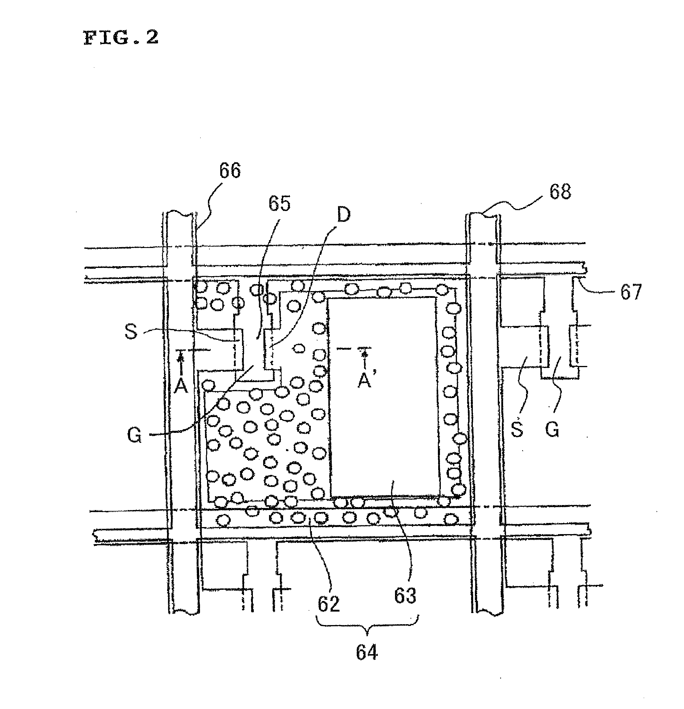
[0092]FIG. 1 is a cross-sectional view showing an essential exemplary structure of a semi-transmissive reflective liquid crystal display apparatus 1 according to an embodiment of the present invention.

[0093]In FIG. 1, the semi-transmissive reflective liquid crystal display app...


PUM

PropertyMeasurementUnit
work functionaaaaaaaaaa

Abstract

A difference of work functions in different metal thin films is suppressed without causing the increase of the manufacturing steps or the decrease of the optical performance. In a semi-transmissive reflective liquid crystal display apparatus 1 including a reflective electrode 62 and a transmissive electrode 63 in the pixel electrode 64, the surface of the reflective electrode 62 is subject to a plasma treatment, so that the work function of the reflective electrode 62 is controlled by changing by a value of 0.1 eV from the original value. Thus, it is possible to place the work function of the reflective electrode 62 within a difference of ±0.2 eV with respect to the work function of the transmissive electrode 63. As a result, a number of the manufacturing steps is not increased or no optical performance is decreased, unlike conventional liquid crystal display apparatuses. Even if the optimum direct current offset voltage is applied to one of the reflective electrode 62 and the transmissive electrode 63, it is possible to reduce the deterioration of an image display quality resulting from the difference with the optimum direct current offset voltage for the other electrode. As such, it is possible to improve the display quality of the liquid crystal display apparatus 1.

Description

TECHNICAL FIELD[0001]The present invention relates to: a metal material and a method for manufacturing the metal material; a thin-film device using the metal material for a metal thin film material and a method for manufacturing the thin-film device; an element-side substrate including a reflective section for producing a reflective display using surrounding light as an illumination, the reflective section including the metal material for a reflective metal electrode, and a transmissive section for producing a transmissive display using backlight as an illumination in one pixel and a method for manufacturing the element-side substrate; and a semi-transmissive reflective liquid crystal display apparatus using the element-side substrate and a method for manufacturing the semi-transmissive reflective liquid crystal display apparatus.BACKGROUND ART[0002]A conventional liquid crystal display apparatus is used for a display section of an electronic information device, such as a cell phone...

Claims


Application Information

Patent Timeline
Patent Type & Authority Applications(United States)
IPC IPC(8): G02F1/1333H05K1/09H01L21/28B05D3/06B32B15/01B32B15/04
CPCC23F4/00G02B5/0808G02F1/133555Y10T428/12493H01L29/458H01L29/66765H01L27/124G02F1/13439
Inventor FUJITA, TETSUOKOKURA, MASAFUMIHARADA, MITSUNORINAKAHARA, HIJIRIKATAOKA, YOSHIHARU
Owner SHARP KK
Why Eureka
Try Eureka