Nonvolatile semiconductor memory device and producing method thereof
- Summary
- Abstract
- Description
- Claims
- Application Information
AI Technical Summary
Problems solved by technology
Method used
Image

Examples
first embodiment
Schematic Configuration of Nonvolatile Semiconductor Memory Device of First Embodiment
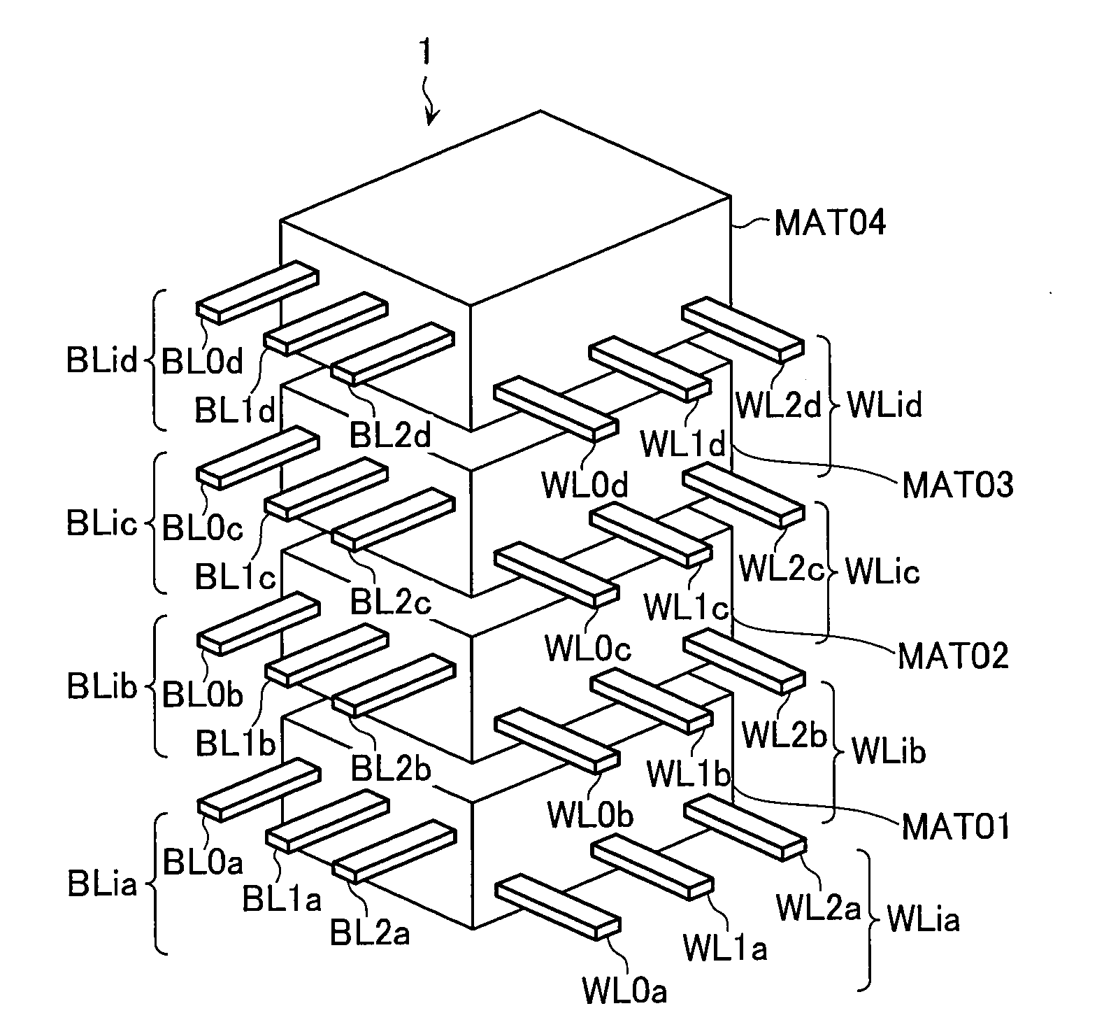
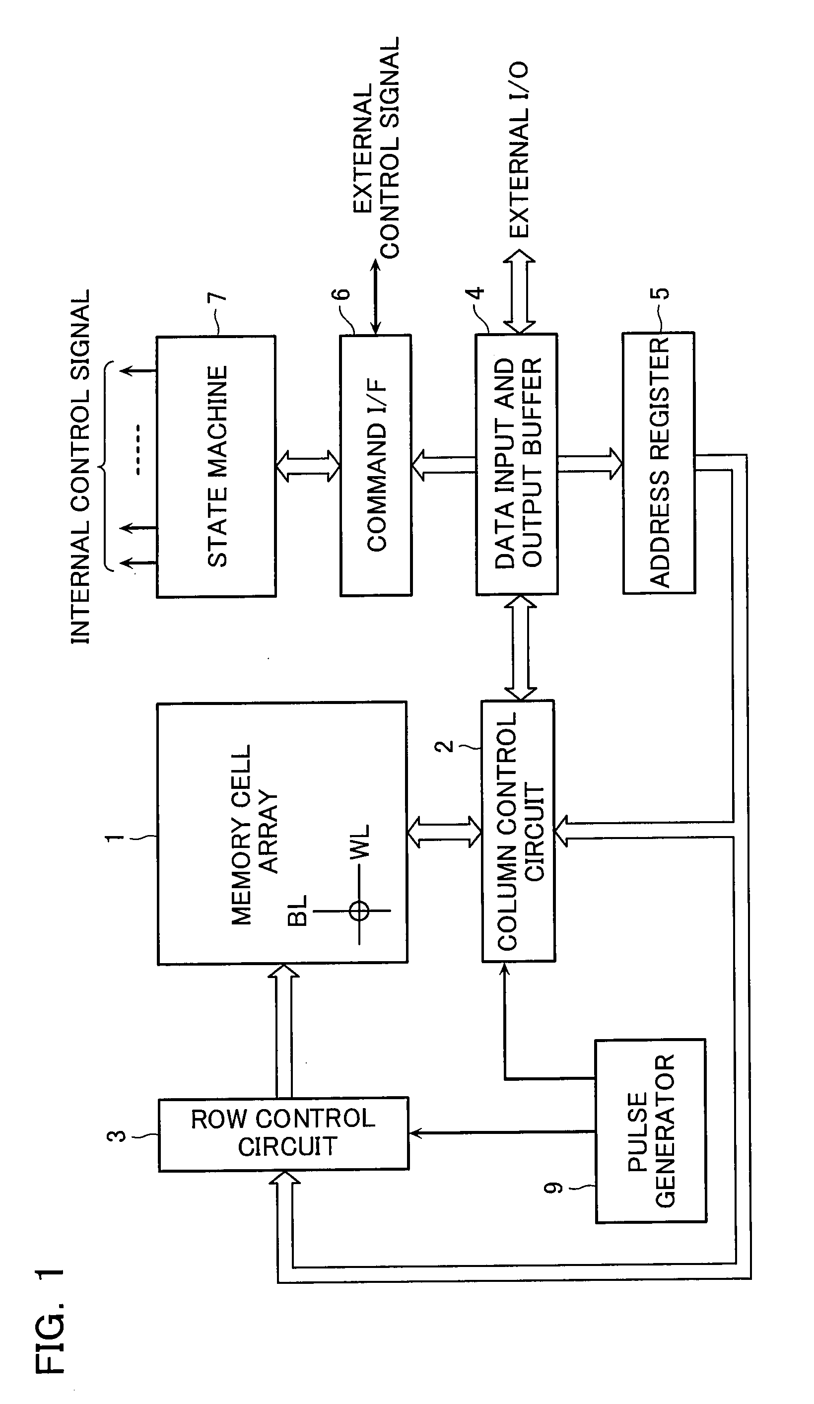
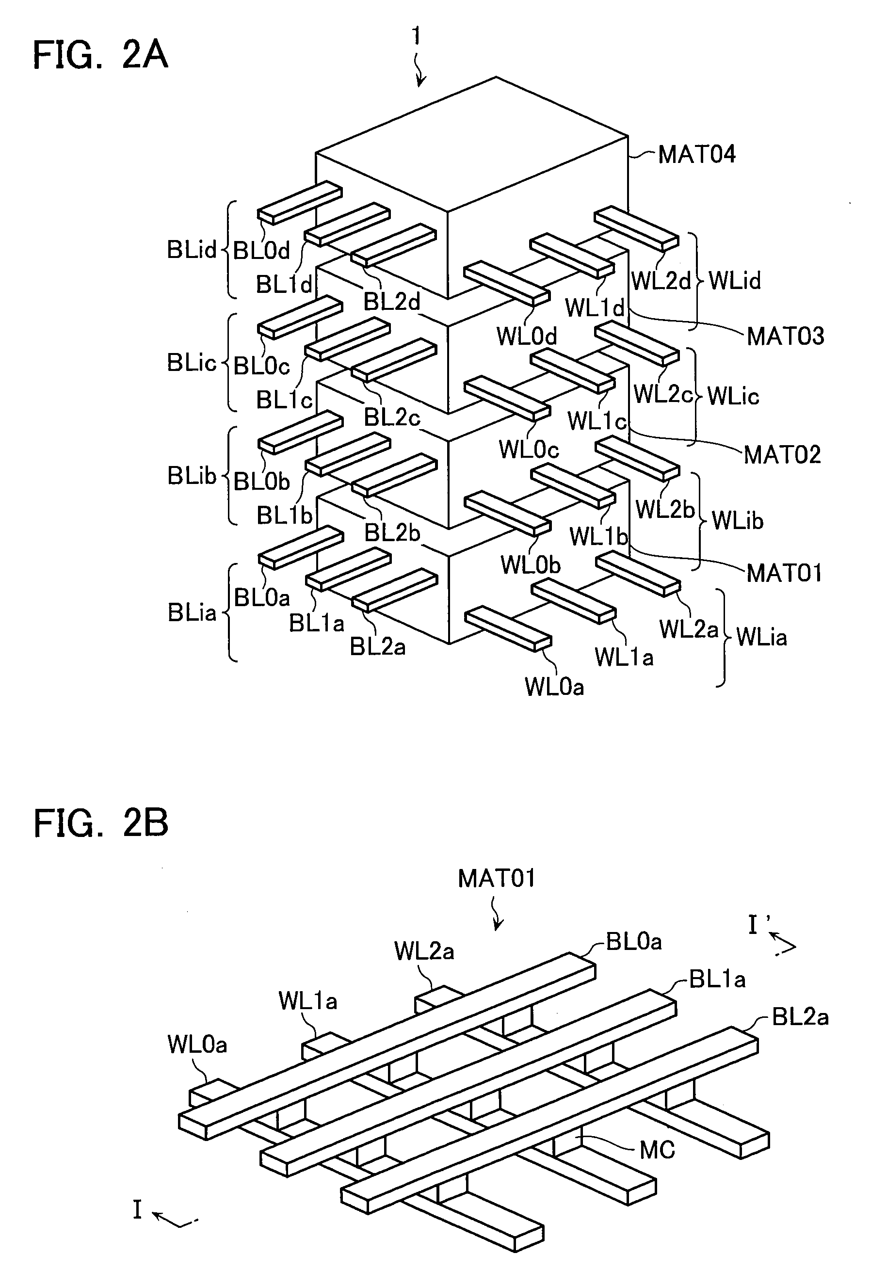
[0067]A schematic configuration of a nonvolatile semiconductor memory device according to a first embodiment of the present invention will be described with reference to FIGS. 1 to 4. FIG. 1 is a block diagram illustrating a nonvolatile semiconductor memory device (nonvolatile memory) of the first embodiment.
[0068]The nonvolatile semiconductor memory device of the first embodiment includes a memory cell array 1 in which memory cells are arranged in a matrix shape, and a later-mentioned ReRAM (variable resistive element) is used in the memory cell. A column control circuit 2 is provided adjacent to the memory cell array 1 in a direction of a bit line BL. The column control circuit 2 controls the bit line BL of the memory cell array 1, erases data of the memory cell, writes the data in the memory cell, and reads the data from the memory cell. A row control circuit 3 is provided adjacent to the memory...
second embodiment
Specific Configuration of Nonvolatile Semiconductor Memory Device of Second Embodiment
[0167]A specific configuration of a nonvolatile semiconductor memory device according to a second embodiment of the present invention will be described with reference to FIGS. 31 and 32. FIG. 31 is a top view illustrating a first metal 27′ and a second metal 36′ of the nonvolatile semiconductor memory device of the second embodiment. FIG. 32 is a view schematically explaining a contact plug of the nonvolatile semiconductor memory device of the second embodiment. In the second embodiment, the same component as the first embodiment is designated by the same numeral, and the description is omitted.
[0168]The nonvolatile semiconductor memory device of the second embodiment includes the first metal 27 similar to that of the first embodiment and a first metal 27′ having a shape different from that of the first embodiment. The nonvolatile semiconductor memory device of the second embodiment includes the se...
third embodiment
Specific Configuration of Nonvolatile Semiconductor Memory Device of Third Embodiment
[0196]A specific configuration of a nonvolatile semiconductor memory device according to a third embodiment of the present invention will be described with reference to FIG. 33. FIG. 33 is a view schematically explaining a contact plug of the nonvolatile semiconductor memory device of the third embodiment. In the third embodiment, the same component as the first and second embodiments is designated by the same numeral, and the description is omitted.
[0197]The nonvolatile semiconductor memory device of the third embodiment is formed with the number of laminated layers different from those of the first and second embodiments. The nonvolatile semiconductor memory device of the third embodiment includes unit cell arrays MAT01′ to MAT04′ different from those of the first and second embodiments.
[0198]Referring to FIG. 33, the upper layer portion is formed on the silicon substrate 51 while roughly includin...
PUM
 Abstract
Description
Claims
Application Information
 - R&D Engineer
- R&D Manager
- IP Professional
- Industry Leading Data Capabilities
- Powerful AI technology
- Patent DNA Extraction
Browse by: Latest US Patents, China's latest patents, Technical Efficacy Thesaurus, Application Domain, Technology Topic.
© 2024 PatSnap. All rights reserved.Legal|Privacy policy|Modern Slavery Act Transparency Statement|Sitemap