Semiconductor storage device having a plurality of stacked memory chips

a memory chip and storage device technology, applied in the field of semiconductor storage devices, can solve the problems of limited storage capacity, low number of memory chips that can be mounted, and the storage capacity required in main memory continues to increase, so as to reduce the number of stacked chips, reduce the number of wires, and reduce the effect of wiring capacitan

Active Publication Date: 2006-10-19
LONGITUDE LICENSING LTD
View PDF13 Cites 282 Cited by
  • Summary
  • Abstract
  • Description
  • Claims
  • Application Information

AI Technical Summary

Benefits of technology

[0018] In the present invention, the single chip that has an interface function may be an interface chip that is different than the plurality of memory chips, or may be any one of the plurality of memory chips. With the former, it is possible to use the exact same chip as the memory chip that is used, and with the latter, it is possible to reduce the number of stacked chips by one.
[0019] The command signals, address signals, and data signals may be transmitted among the plurality of memory chips and the single chip that has an interface function by way of wiring with a shared connection to the plurality of memory chips, or may be carried out by way of wiring that is individually connected to the plurality of memory chips. The former allows the number of wires to be reduced, and the latter allows the wiring capacitance to be reduced.
[0020] Thus, in accordance with the present invention, it is possible to reduce the parasitic capacitance of the interface unit of a semiconductor storage device having a plurality of stacked memory chips to an amount equal to that of a single chip component. The input/output frequency of the command signal

Problems solved by technology

Semiconductor storage devices typified by DRAM (Dynamic Random Access Memory) are widely used as the main memory of servers and other computers, but with the increase in hardware speed and software complexity, the storage capacity required in main memory continues to increase.
However, the number of memory chips that can be mounted is low and the resulting storage capacity is limited when the memory chip is disposed in a flat configuration on a module substrate.
However, since the semiconductor storage device shown in FIG. 22 is configured so that the command/address external terminal group CA and data input/output external terminal group DQ are connected to the memory chips 10 and 11, there is a problem in that the parasitic capacitance of the command/address external terminal group CA and the data input/output external terminal group DQ is considerable in comparison with ordinary semiconductor storage devices in which only a single chip has been packaged.
Since such parasitic capacitance is the cause of signal waveform disturbance, there is a possibility that an ade

Method used


Image

  • Semiconductor storage device having a plurality of stacked memory chips
  • Semiconductor storage device having a plurality of stacked memory chips
  • Semiconductor storage device having a plurality of stacked memory chips

Examples


first embodiment

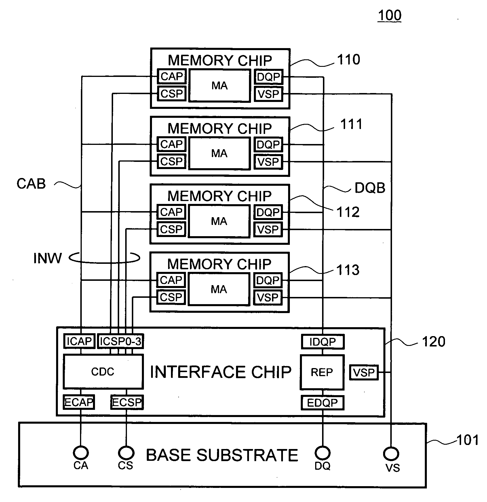
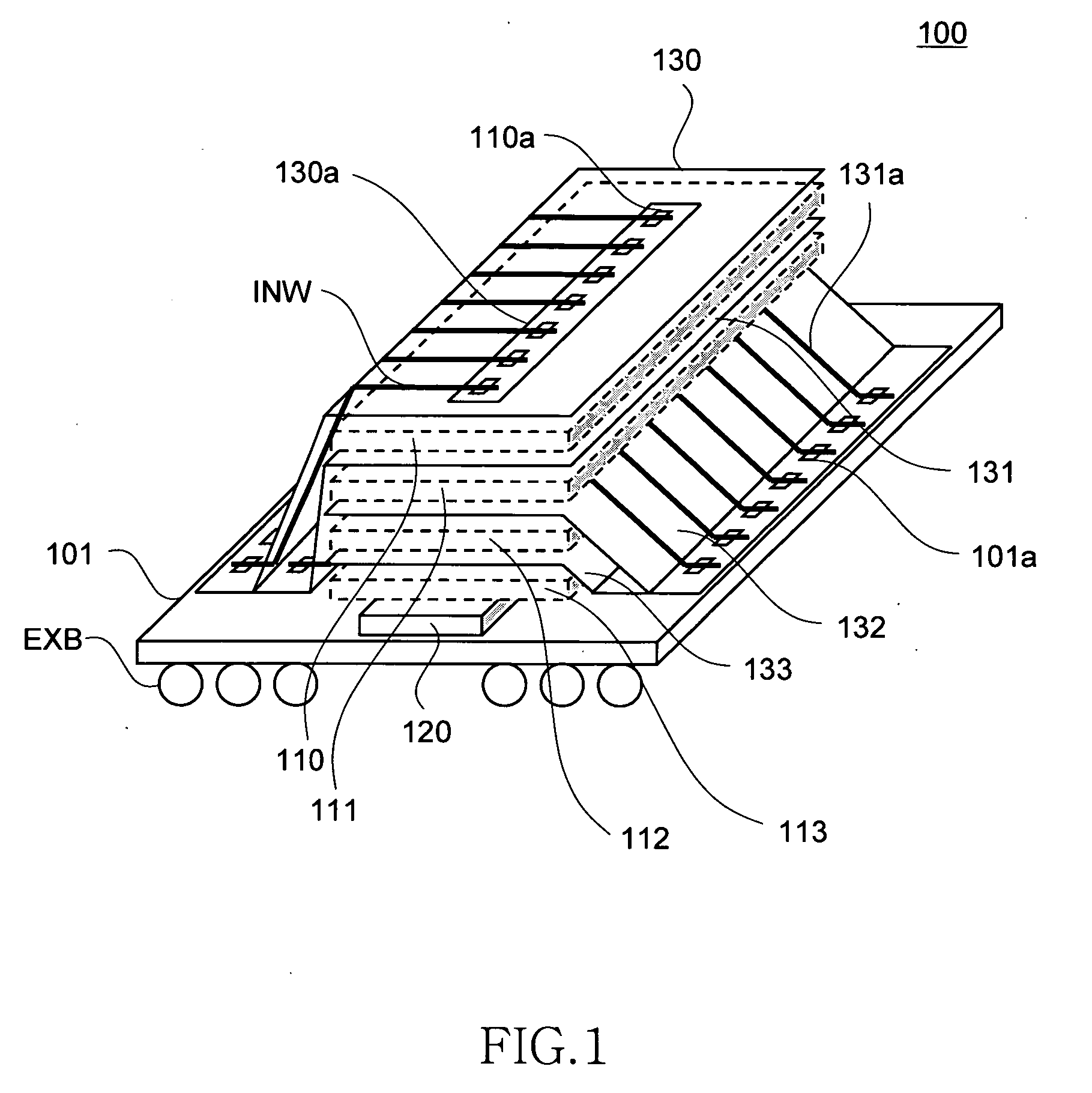
[0049]FIG. 1 is a simplified perspective view that schematically shows the structure of the semiconductor storage device 100 according to the present invention.

[0050] The semiconductor storage device 100 of the present embodiment is provided with a base substrate 101, four memory chips 110 to 113 stacked on the base substrate 101, and an interface chip 120 disposed between the base substrate 101 and memory chips 110 to 113, as shown in FIG. 1. In the present embodiment, DRAM is selected as the memory chips 110 to 113, although this selection imposes no particular limitation. The memory chips 110 to 113 are chips having mutually the same configuration, and are DRAM chips that are individually capable of read and write operations, that is to say, the chips are ordinary general-purpose DRAM chips.

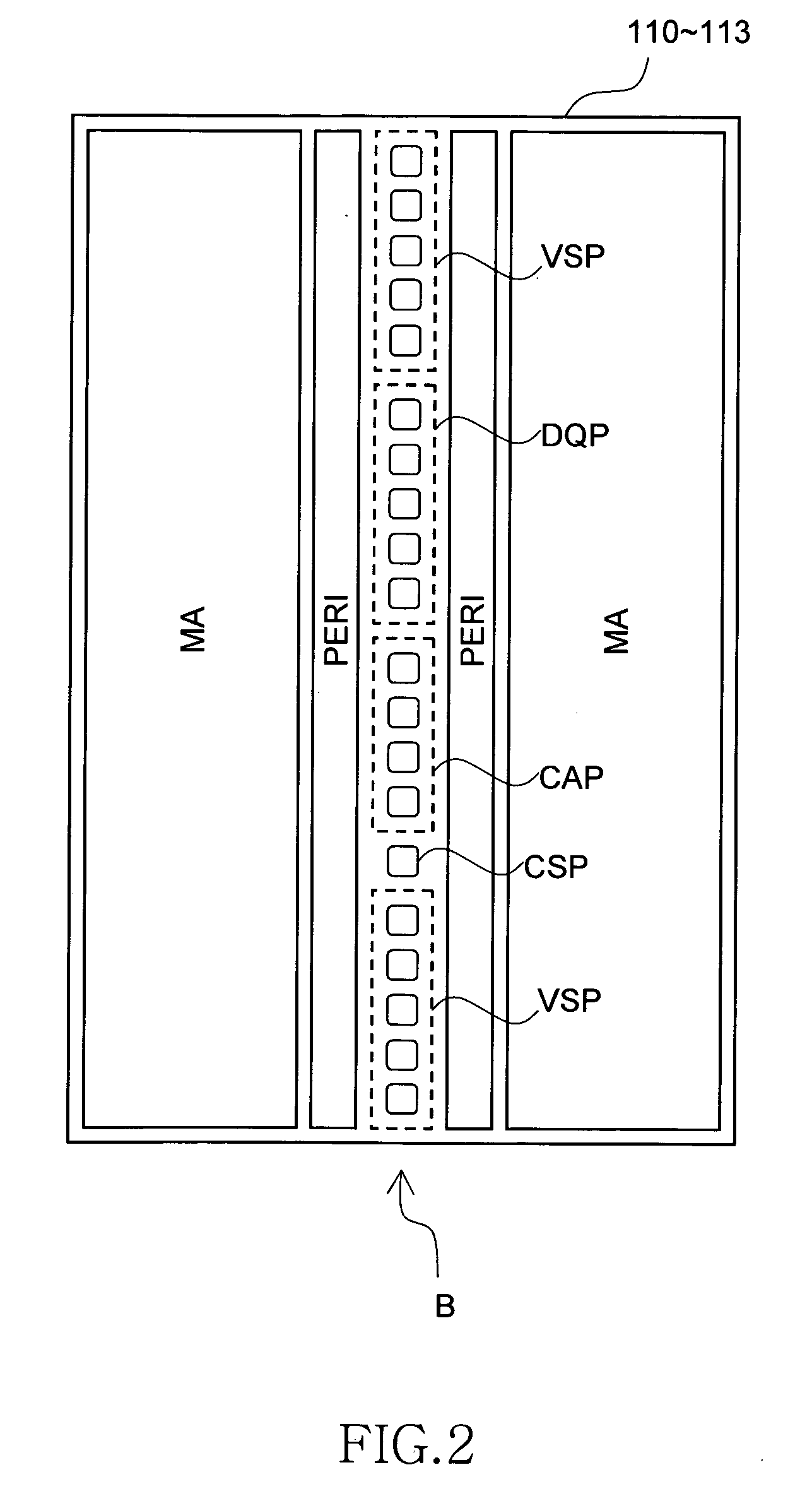
[0051]FIG. 2 is a simplified planar view of the memory chips 110 to 113.

[0052] The surface of the memory chips 110 to 113 can be largely classified into a memory array area MA, a peripheral ...

third embodiment

[0157]FIG. 21 is a schematic diagram that describes the connection configuration between the memory chips 110 to 112 and the memory chip 320 in the semiconductor storage device 300 of the present invention.

[0158] In the present embodiment, the special-purpose interface chip is dispensed with. Instead, an interface chip function is provided to the memory chip 320 that is most proximate to the base substrate 101, as shown in FIG. 21. Other than the above, the configuration is the same as the semiconductor storage device 100 of the first embodiment described above. Signals other than the chip select signals CS0 to CS2 are bus-connected using the command / address bus CAB and the data bus DQB between the memory chips 110 to 112 and the memory chip 320. According to the present invention, the number of chips can be reduced by one, and the thickness of the entire package can therefore be reduced. Also, since the number of wires and the load of the internal wiring INW can be reduced, power c...


PUM


Abstract

A semiconductor storage employs a base substrate (101) having a command/address external terminal group (CA), a data input/output external terminal group (DQ), and a single chip select external terminal (CS), and also comprises a plurality of memory chips (110) to (113) mounted on a base substrate (101), each of which can individually carry out read and write operations. The terminals (CA), (DQ), and (CS) are connected to an interface chip (120). The interface chip (120) has a chip select signal generation circuit that can individually activate a plurality of memory chips (110) to (113) on the basis of an address signal fed by way of the terminal (CA) and on the basis of a chip select signal fed by way of the terminal (CS).

Description

TECHNICAL FIELD [0001] The present invention relates to a semiconductor storage device, and more specifically relates to a semiconductor storage device that has a plurality of stacked memory chips. BACKGROUND OF THE INVENTION [0002] Semiconductor storage devices typified by DRAM (Dynamic Random Access Memory) are widely used as the main memory of servers and other computers, but with the increase in hardware speed and software complexity, the storage capacity required in main memory continues to increase. For this reason, it is difficult to meet the storage capacity needs required in main memory by using only a single memory chip, and a module referred as DIMM (Dual Inline Memory Module) in which a plurality of memory chips are mounted on a module substrate is ordinarily used. [0003] However, the number of memory chips that can be mounted is low and the resulting storage capacity is limited when the memory chip is disposed in a flat configuration on a module substrate. Methods have ...

Claims


Application Information

Patent Timeline
IPC IPC(8): G11C5/02
CPCG11C5/02G11C5/04H01L24/50G11C11/4074G11C11/4096G11C8/12
Inventor SEKIGUCHI, TOMONORIOSAKA, HIDEKIIDO, TATEMINAGASHIMA, OSAMUKATAGIRI, MITSUAKIANJO, ICHIRO
Owner LONGITUDE LICENSING LTD
Why Eureka
Try Eureka