Integrating the Formation of I/O and Core MOS Devices with MOS Capacitors and Resistors

a technology of mos capacitors and resistors, applied in the direction of diodes, capacitors, semiconductor devices, etc., can solve the problems of significantly changing the electrical properties of these devices, depleting polysilicon, and high cost and time consumption, and achieve the effect of reducing complexity and cos

Active Publication Date: 2010-02-18
TAIWAN SEMICON MFG CO LTD
View PDF37 Cites 52 Cited by
  • Summary
  • Abstract
  • Description
  • Claims
  • Application Information

AI Technical Summary

Benefits of technology

[0012]The embodiments of the present invention provide an integrated manufacturing process for forming resistors, MOS capacitors, I / O MOS devices, SRAM MOS devices, and core MOS devices with reduced complexity and cost. By using the embodiments of the present invention, conventional standard libraries for resistors, MOS capacitors can continuously be used.

Problems solved by technology

However, polysilicon has depletion problems, and hence metal gate electrodes were introduced, particularly for MOS device in core regions, to avoid the poly depletion phenomenon.
This significantly changes the electrical properties of these devices.
The standard libraries built in the past decades for simulating the behavior of these devices thus have to be rebuilt, which is highly costly and time consuming.
However, the manufacturing schemes for forming such structures are often complicated, and the manufacturing cost is high.

Method used


Image

  • Integrating the Formation of I/O and Core MOS Devices with MOS Capacitors and Resistors
  • Integrating the Formation of I/O and Core MOS Devices with MOS Capacitors and Resistors
  • Integrating the Formation of I/O and Core MOS Devices with MOS Capacitors and Resistors

Examples


Embodiment Construction

[0016]The making and using of the presently preferred embodiments are discussed in detail below. It should be appreciated, however, that the present invention provides many applicable inventive concepts that can be embodied in a wide variety of specific contexts. The specific embodiments discussed are merely illustrative of specific ways to make and use the invention, and do not limit the scope of the invention.

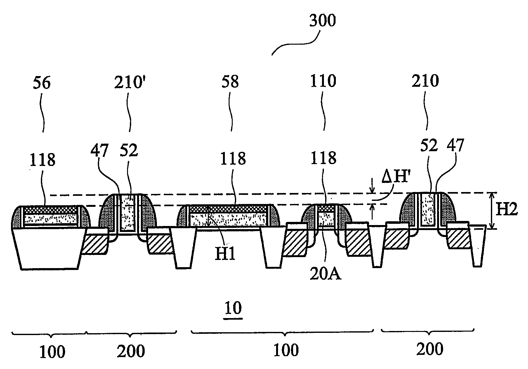
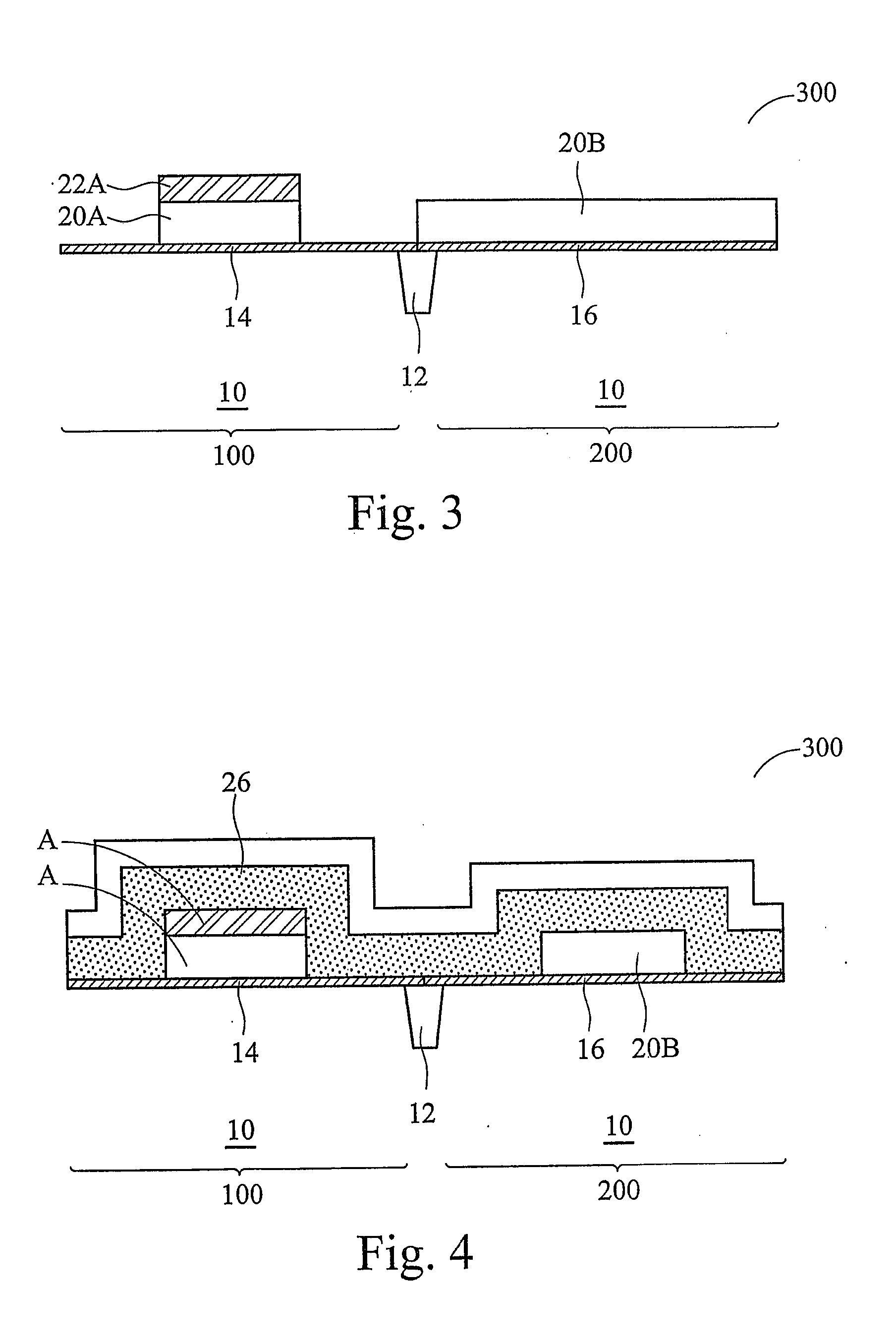
[0017]An integration scheme integrating the manufacture of core metal-oxide-semiconductor (MOS) devices, input / output (I / O) MOS device, static random access memory (SRAM) MOS devices, resistors, MOS capacitors, and the like, is provided. The intermediate stages of manufacturing preferred embodiments of the present invention are illustrated. The variations of the preferred embodiments are then discussed. Throughout the various views and illustrative embodiments of the present invention, like reference numbers are used to designate like elements.

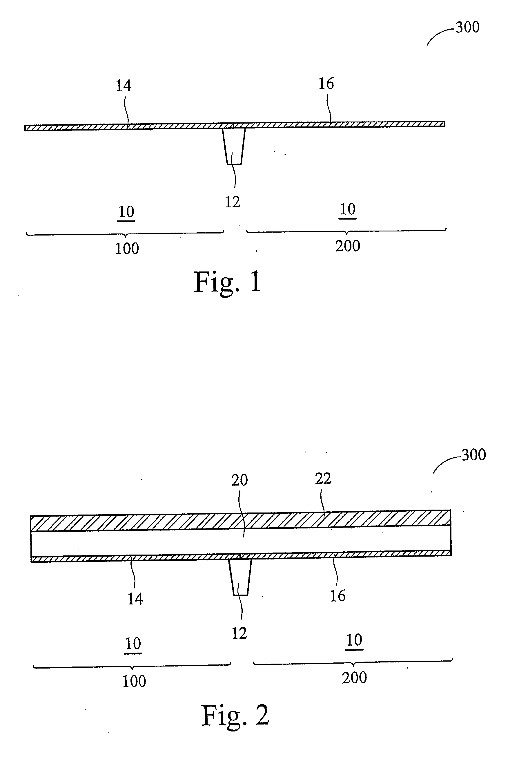
[0018]Referring to FIG. 1, semic...


PUM


Abstract

An integrated circuit structure includes a semiconductor substrate, and a first and a second MOS device. The first MOS device includes a first gate dielectric over the semiconductor substrate, wherein the first gate dielectric is planar; and a first gate electrode over the first gate dielectric. The second MOS device includes a second gate dielectric over the semiconductor substrate; and a second gate electrode over the second gate dielectric. The second gate electrode has a height greater than a height of the first gate electrode. The second gate dielectric includes a planar portion underlying the second gate electrode, and sidewall portions extending on sidewalls of the second gate electrode.

Description

TECHNICAL FIELD[0001]This invention relates generally to integrated circuits, and more particularly to the formation of metal-oxide-semiconductor (MOS) devices having polysilicon gates and MOS devices having metal gates.BACKGROUND[0002]Complementary metal-oxide-semiconductor (MOS) devices have been the basic logic building blocks in the formation of integrated circuits. In traditional IC processes, gate electrodes are typically formed of polysilicon. One of the reasons for polysilicon's wide use is that the work function of polysilicon gate electrodes can be changed easily by doping with different impurities. However, polysilicon has depletion problems, and hence metal gate electrodes were introduced, particularly for MOS device in core regions, to avoid the poly depletion phenomenon.[0003]With the adoption of metal gates, naturally, core MOS devices, input / output (I / O) MOS devices, and static random access memory (SRAM) MOS devices may all have metal gates, so that they can be manu...

Claims


Application Information

Patent Timeline
Patent Type & Authority Applications(United States)
IPC IPC(8): H01L27/11
CPCH01L27/0629H01L27/105H01L27/11H01L29/94H01L28/20H01L28/40H01L27/1116H10B10/00H10B10/18
Inventor CHUANG, HARRYLIANG, MONG SONGYANG, WEN-CHIHCHEN, CHIEN-LIANGLI, CHII-HORNG
Owner TAIWAN SEMICON MFG CO LTD
Why Eureka
Try Eureka