Plasma display device and method for driving plasma display panel
a display device and plasma technology, applied in the direction of instruments, computing, electric digital data processing, etc., can solve the problems of increasing the applied voltage, affecting and unstable address, so as to improve the quality of image display and generate stably
- Summary
- Abstract
- Description
- Claims
- Application Information
AI Technical Summary
Benefits of technology
Problems solved by technology
Method used
Image

Examples
first exemplary embodiment
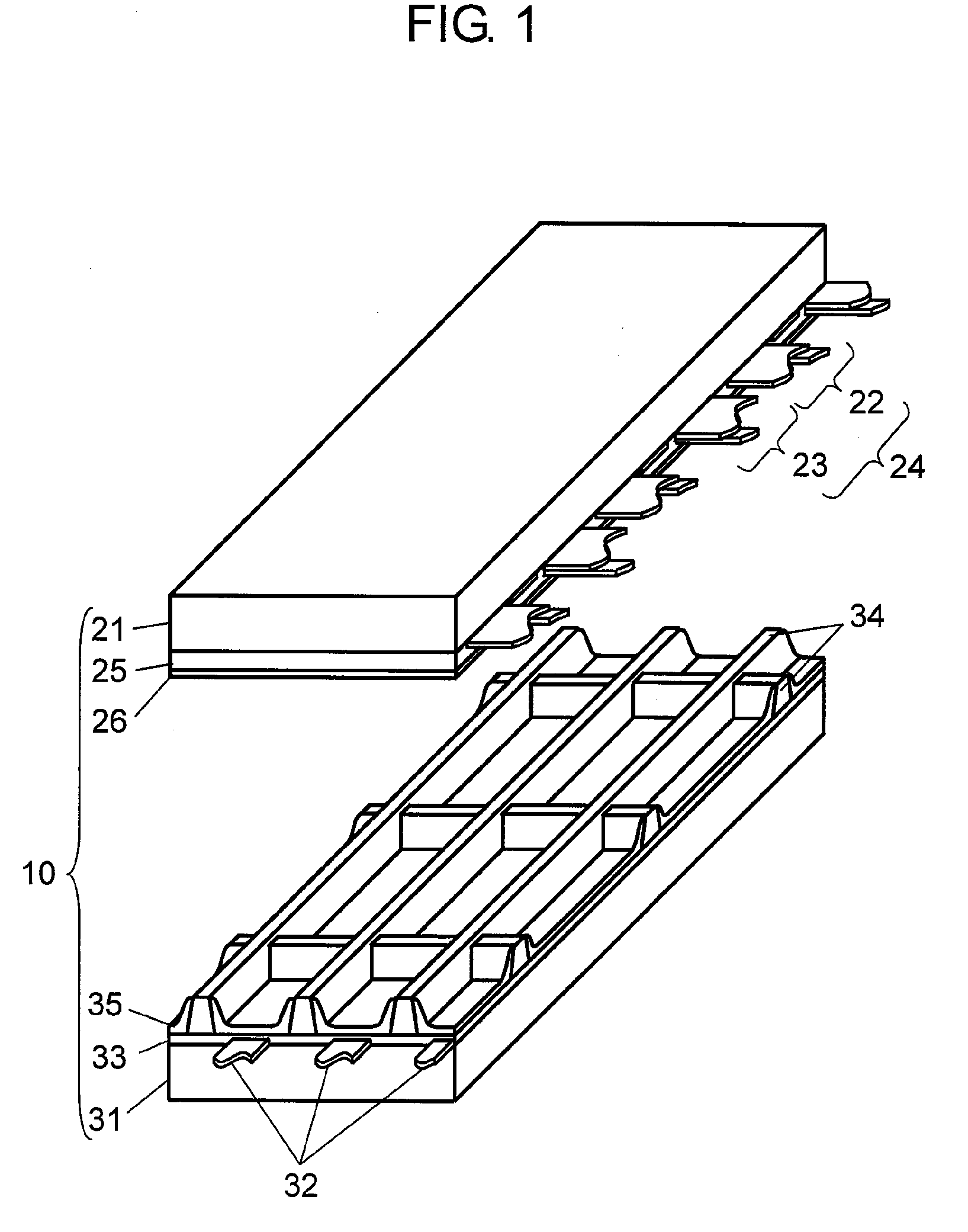
[0080]FIG. 1 is an exploded perspective view showing a structure of panel 10 in accordance with the first exemplary embodiment of the present invention. A plurality of display electrode pairs 24 each composed of scan electrode 22 and sustain electrode 23 are formed on glass front panel 21. Dielectric layer 25 is formed so as to cover scan electrode 22 and sustain electrode 23. Protective layer 26 is formed on dielectric layer 25.
[0081]Furthermore, protective layer 26 is made of a material containing MgO as a main component, which has been used as a panel material in order to reduce a discharge start voltage in the discharge cell, has a large secondary electron emission coefficient when neon (Ne) and xenon (Xe) gasses are filled and is excellent in durability.
[0082]A plurality of data electrodes 32 are formed on rear panel 31, dielectric layer 33 is formed so as to cover data electrodes 32, and further double-cross-shaped barrier ribs 34 are formed on dielectric layer 33. Phosphor la...
second exemplary embodiment
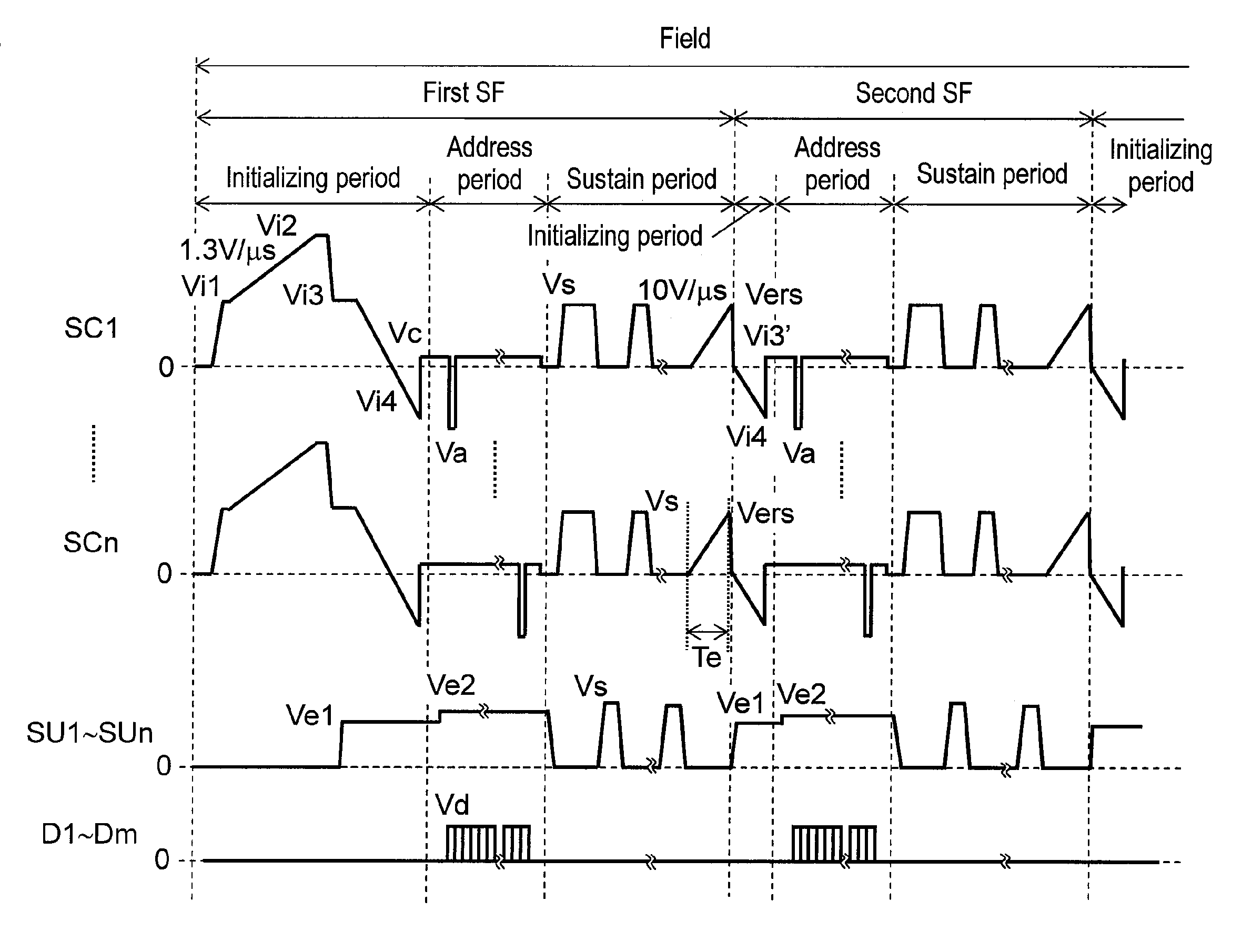
[0209]The first exemplary embodiment 1 is characterized in that initializing voltage Vi4 is switched at Vi4L, Vi4M and Vi4H for every subfield according to the total number of sustain pulses in the sustain period and the temperature of panel 10. However, the second exemplary embodiment is characterized in that initializing voltage Vi4 is switched at Vi4L, Vi4M and Vi4H according to only the total number of sustain pulses of the sustain period. Therefore, the description of the configuration and operation that are the same as those in the first exemplary embodiment is omitted herein.
[0210]FIG. 15 shows one example of a configuration of a subfield in accordance with the second exemplary embodiment of the present invention. For example, as shown in FIG. 15, regardless of the temperature of the panel, in the initializing period of a subfield in which the total number of sustain pulses in the immediately preceding subfield is less than 20 (herein, second SF to fourth SF) and in the initi...
third exemplary embodiment
[0211]The first exemplary embodiment is characterized in that initializing voltage Vi4 is switched at Vi4L, Vi4M and Vi4H for every subfield according to the total number of sustain pulses in the sustain period and the temperature of panel 10. However, the third exemplary embodiment is characterized in that initializing voltage Vi4 is switched at Vi4L, Vi4M and Vi4H according to only the temperature of panel 10. Therefore, the description of the configuration and operation that are the same as those in the first exemplary embodiment is omitted herein.
[0212]FIGS. 16A, 16B and 16C are views showing one example of the subfield configuration in the third exemplary embodiment of the present invention. For example, when panel temperature detecting circuit 46 determines that the temperature of panel 10 is a high temperature (not less than 55° C.), as shown in FIG. 16A, initializing voltage Vi4 is set to Vi4H in the initializing period of all the subfields to generate a downward ramp wavefo...
PUM
 Abstract
Description
Claims
Application Information
 - Generate Ideas
- Intellectual Property
- Life Sciences
- Materials
- Tech Scout
- Unparalleled Data Quality
- Higher Quality Content
- 60% Fewer Hallucinations
Browse by: Latest US Patents, China's latest patents, Technical Efficacy Thesaurus, Application Domain, Technology Topic, Popular Technical Reports.
© 2025 PatSnap. All rights reserved.Legal|Privacy policy|Modern Slavery Act Transparency Statement|Sitemap|About US| Contact US: help@patsnap.com