Nonvolatile semiconductor device and method of manufacturing nonvolatile semiconductor device

a nonvolatile semiconductor and nonvolatile technology, applied in the direction of semiconductor devices, electrical devices, transistors, etc., can solve the problems of inhibiting the function of the nonvolatile semiconductor device, difficult capacitive coupling between adjacent floating gates, etc., and achieve the effect of suppressing the fluctuation of the threshold voltage of the floating ga

Inactive Publication Date: 2010-02-25
RENESAS ELECTRONICS CORP
View PDF9 Cites 19 Cited by
  • Summary
  • Abstract
  • Description
  • Claims
  • Application Information

AI Technical Summary

Benefits of technology

[0014]According to a nonvolatile semiconductor device and a method of manufacturing the same according to the present invention, a variation in a threshold voltage of a floating gate can be suppressed while ensuring a function of the nonvolatile semiconductor device.

Problems solved by technology

With this, suppression of capacitive coupling between adjacent floating gates becomes difficult and a threshold voltage of a selected floating gate varies.
Furthermore, in a nonvolatile semiconductor device having low-permittivity films having a permittivity lower than that of a silicon oxide film which are formed between floating gates and between control gates, hydrogen or water may exude to a gate insulation film, which inhibits a function of the nonvolatile semiconductor device.

Method used


Image

  • Nonvolatile semiconductor device and method of manufacturing nonvolatile semiconductor device
  • Nonvolatile semiconductor device and method of manufacturing nonvolatile semiconductor device
  • Nonvolatile semiconductor device and method of manufacturing nonvolatile semiconductor device

Examples


first embodiment

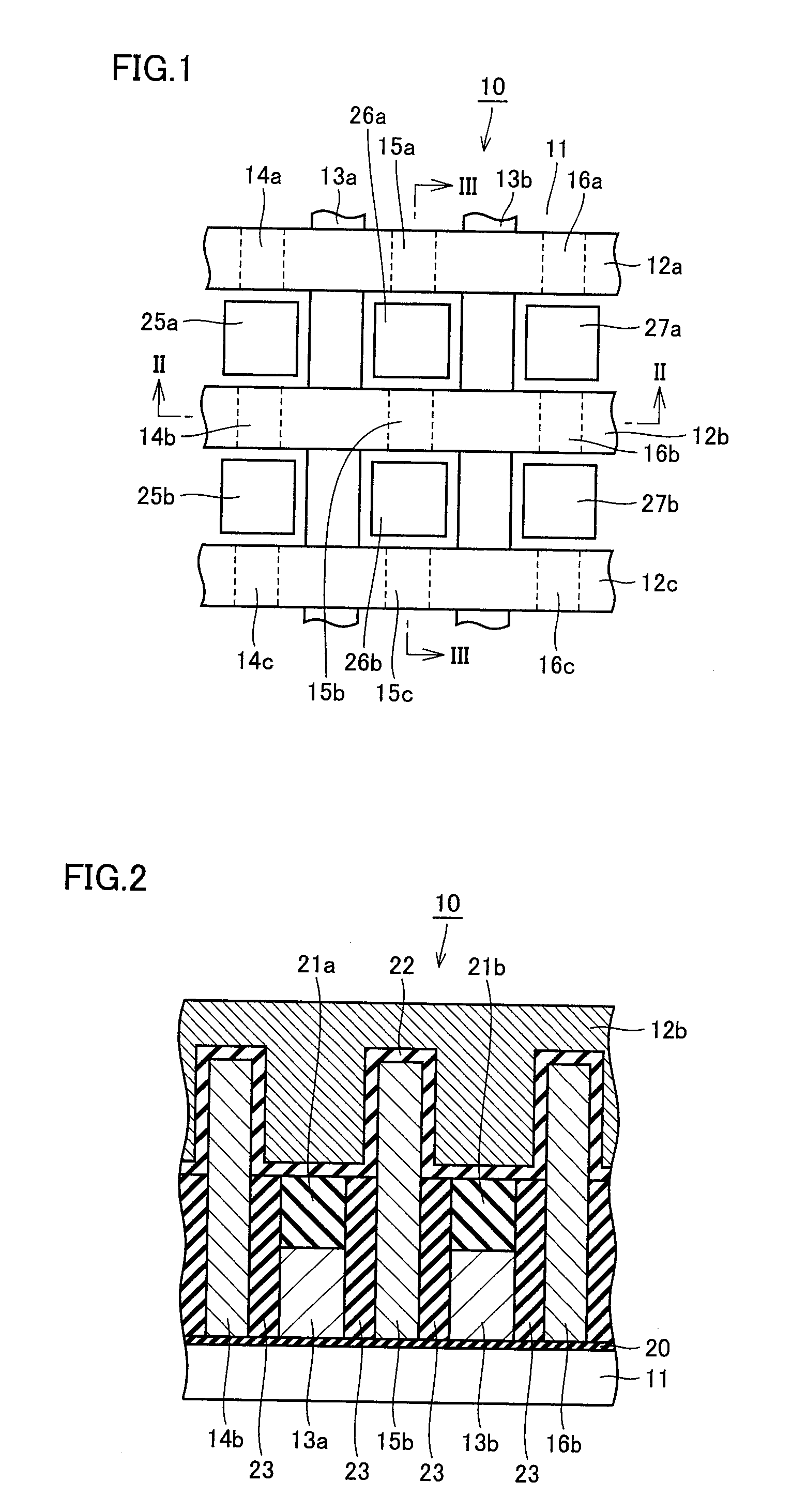
[0028]FIG. 1 is a plan view of a nonvolatile semiconductor device 10 according to a first embodiment. As shown in FIG. 1, a semiconductor substrate 11 having a main surface, assist gates 13a, 13b formed spaced apart from each other on the main surface of semiconductor substrate 11 and extending in one direction, floating gates (first floating gates) 14a-16a, 14c-16c formed on the main surface of semiconductor substrate 11, and floating gates (second floating gates) 14b-16b formed spaced apart from floating gates 14a-16a, 14c-16c are included.

[0029]Nonvolatile semiconductor device 10 also includes control gates (first control gates) 12a, 12c formed on floating gates 14a-16a, 14c-16c, and a control gate (second control gate) 12b formed on floating gates 14b-16b.

[0030]A plurality of floating gates 15a-15c are formed spaced apart from each other between assist gates 13a, 13b along an extending direction of assist gates 13a, 13b. In addition, gap portions 25a-27a, 25b-27b are formed bet...

second embodiment

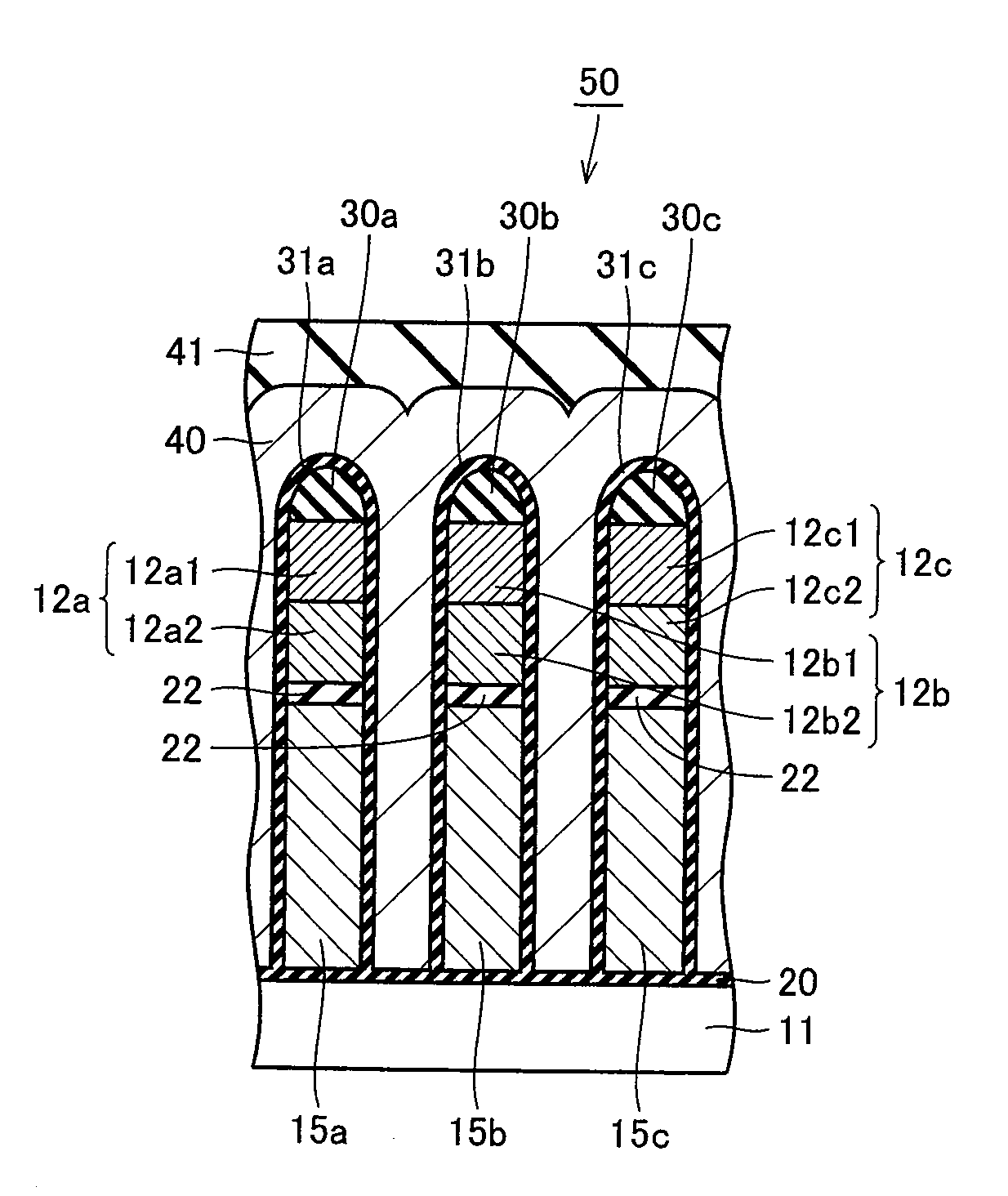
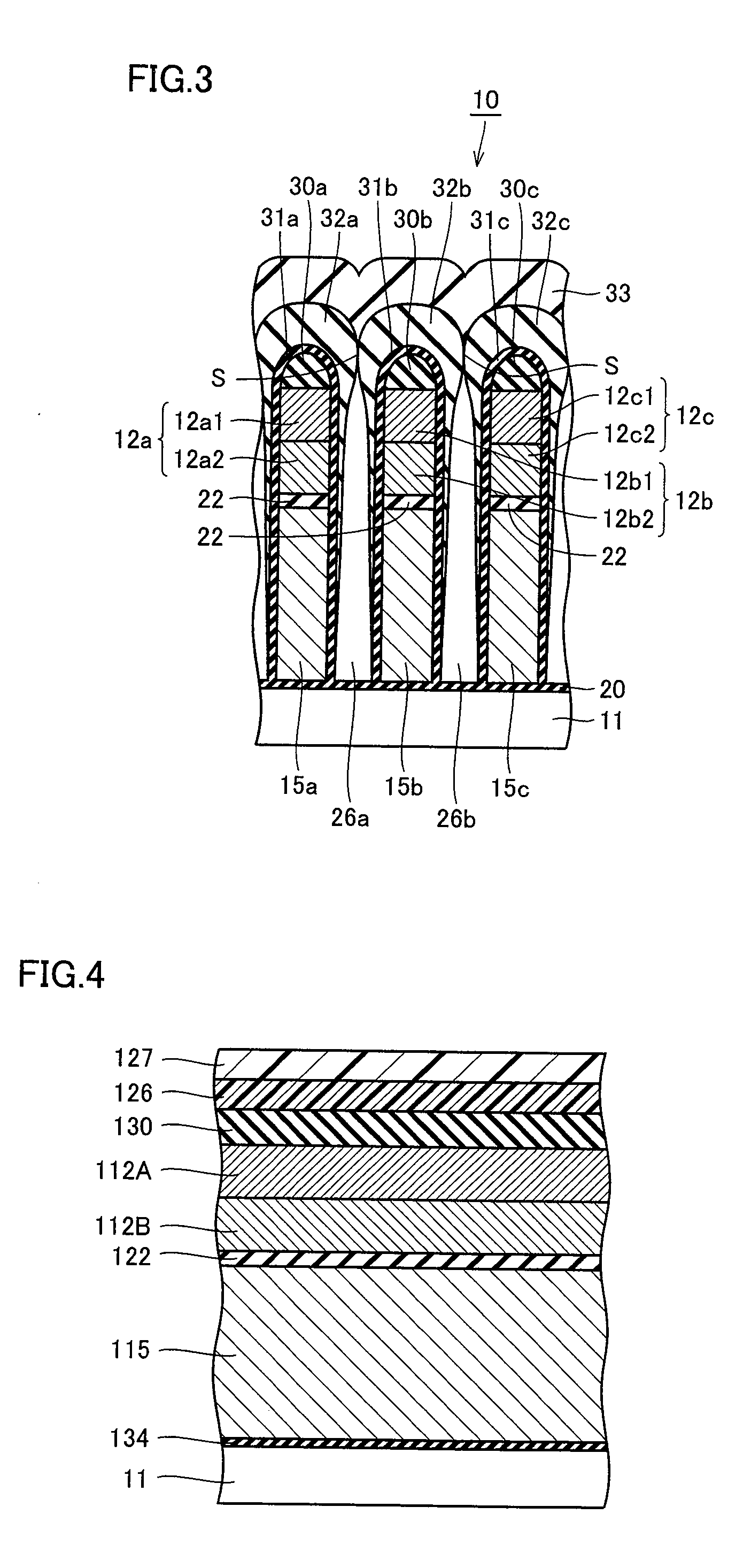
[0064]A nonvolatile semiconductor device 50 according to a second embodiment will now be described using FIGS. 10-17. FIG. 10 is a cross-sectional view of nonvolatile semiconductor device 50 according to the second embodiment. As shown in FIG. 10, nonvolatile semiconductor device 50 includes insulation film 20 formed on the main surface of semiconductor substrate 11, floating gates 15a-15c formed on the main surface via insulation film 20, ONO film 22 formed on top surfaces of floating gates 15a-15c, and control gates 12a-12c respectively formed on floating gates 15a-15c via ONO film 22.

[0065]Nonvolatile semiconductor device 50 also includes an insulation film 40 formed between control gates 12a-12c and between floating gates 15a-15c. Insulation film 40 is a porous insulation film having a permittivity lower than that of a silicon oxide film. A porous film having a permittivity of about 2.6, more specifically, silsesquioxane, porous silica, an aerogel thin film, HSG-255 (an organic ...


PUM


Abstract

A semiconductor substrate having a main surface, first and second floating gates formed spaced apart from each other on the main surface of the semiconductor substrate, first and second control gates respectively located on the first and second floating gates, a first insulation film formed on the first control gate, a second insulation film formed on the second control gate to contact the first insulation film, and a gap portion formed at least between the first floating gate and the second floating gate by achieving contact between the first insulation film and the second insulation film are included. With this, a function of a nonvolatile semiconductor device can be ensured and a variation in a threshold voltage of a floating gate can be suppressed.

Description

BACKGROUND OF THE INVENTION[0001]1. Field of the Invention[0002]The present invention relates to a nonvolatile semiconductor device having reduced capacitive coupling between floating gates and a method of manufacturing the same.[0003]2. Description of the Background Art[0004]A generally known nonvolatile semiconductor device allowing electrical writing and erasing includes a plurality of floating gate electrodes formed on a main surface of a semiconductor substrate and control gate electrodes formed on the floating gate electrodes. As a degree of integration of a semiconductor integrated circuit becomes higher in recent years, a dimension between floating gates becomes smaller and a large capacity is readily generated between adjacent floating gates. As a result, a problem due to so-called capacitive coupling occurs, that is, a threshold voltage during reading of the floating gate varies according to potentials of surrounding floating gates.[0005]Therefore, a nonvolatile semiconduc...

Claims


Application Information

Patent Timeline
Patent Type & Authority Applications(United States)
IPC IPC(8): H01L29/788
CPCH01L21/7682H01L29/42324H01L29/40114H10B69/00H10B41/30
Inventor YONEMOCHI, YASUAKIOTOI, HISAKAZUNISHIDA, AKIOSHIRATAKE, SHIGERU
Owner RENESAS ELECTRONICS CORP
Why Eureka
Try Eureka