Lithium niobate modulator having a doped semiconductor structure for the mitigation of DC bias drift

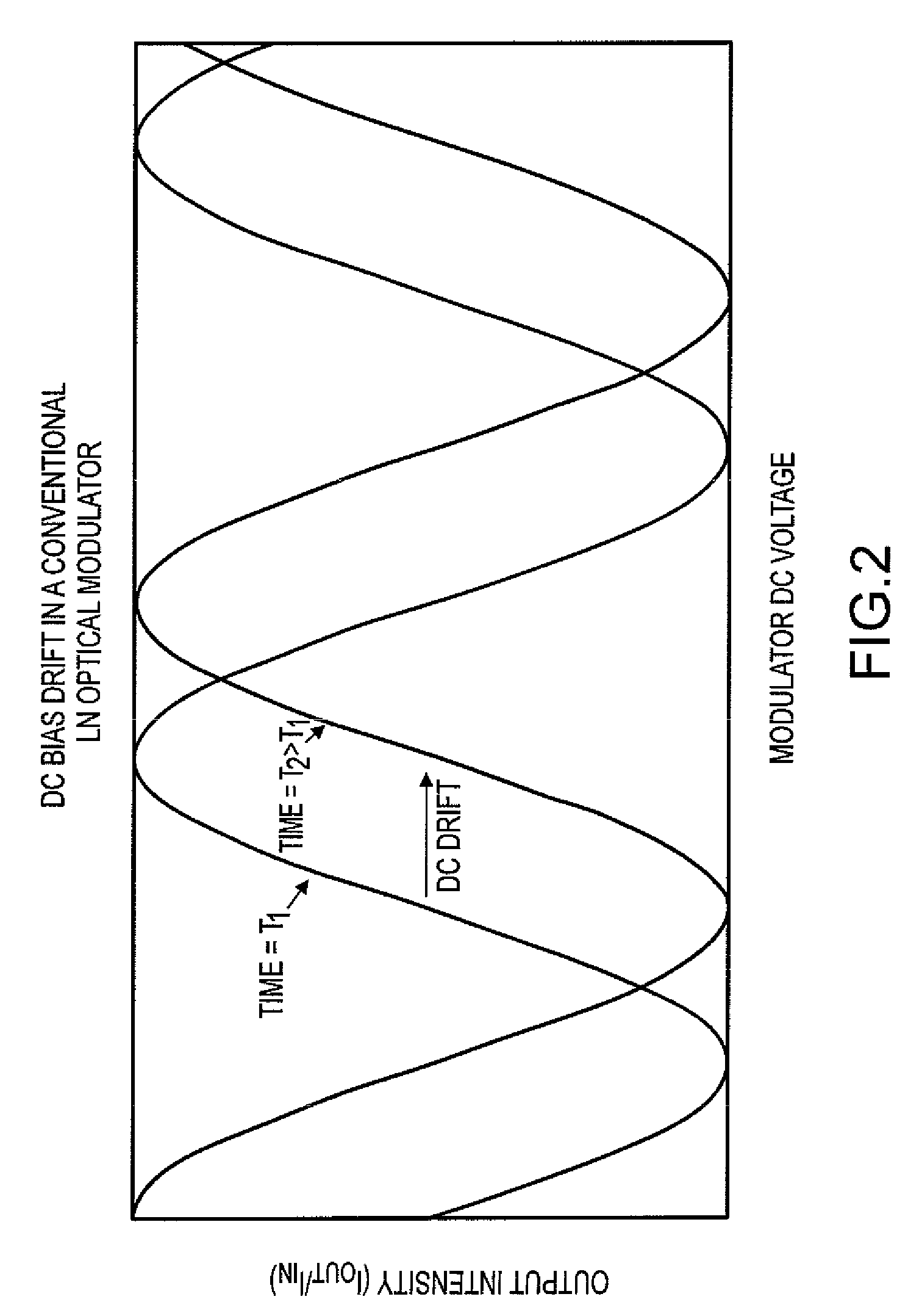
a technology of lithium niobate and electrooptical modulators, which is applied in the field of lithium niobate electrooptical modulators having a doped semiconductor structure for the mitigation can solve the problems of dc (direct current) bias drift, loss of data, phase shift of relative intensity, etc., and achieves predictability and reliable solutions. , the effect of reducing the probability of dc bias dri

Inactive Publication Date: 2010-02-25
THE BOEING CO
View PDF8 Cites 2 Cited by
  • Summary
  • Abstract
  • Description
  • Claims
  • Application Information

AI Technical Summary

Benefits of technology

[0007]This need for an LN electro-optical modulator having a doped semiconductor structure for the mitigation of DC bias drift, as well as a unique, nonobvious, and advantageous method and system, is satisfied and numerous advantages are discussed herein. Embodiments of the LN electro-optical modulator having a doped semiconductor structure for the mitigation of DC bias drift may provide one or more of the following advantages: provides an LN electro-optical modulator device that gives a predictable and reliable solution for the mitigation of DC bias drift; provides an LN electro-optical modulator structure that mitigates DC bias drift and is simple to implement; provides an LN electro-optical modulator device that is fabricated with a buffer layer only in the RF section and not in the DC sections of the device, thus eliminating a conventional (0.5-1.0 μm (micrometer) thick) oxide buffer layer from the DC sections of the device, which in turn, reduces the DC switching voltage (Vπ); provides an LN electro-optical modulator device that eliminates irreproducibility issues by applying the bias voltage directly to the optical waveguide structure; provides an LN electro-optical modulator having a highly doped semiconductor layer on top of the optical waveguide that is electrically contacted by a metal or conductive layer at a point outside the waveguide, thus creating a good contact to allow uniform distribution of the electric field; provides an LN electro-optical modulator device that is simple to construct and is robust and reproducible; provides an LN electro-optical modulator device that minimizes having to use a feedback loop to monitor DC bias drift; provides a method of mitigating DC bias drift using an LN electro-optical modulator as described herein; and provides an LN electro-optical modulator device that can be used in numerous applications including, but not limited to, long distance communication systems, such as free space laser communication systems for satellite and terrestrial applications, and terrestrial and underwater fiber optic communication.

Problems solved by technology

An occurrence associated with known LN electro-optical modulators is the occurrence of DC (Direct Current) bias drift caused by undesirable charge generation and charge redistribution in the device.
DC bias drift is a change in the output voltage of a power supply used to bias the modulator at a certain operating point, over a certain period of time, Steady increases to the voltage required to maintain the bias condition can cause a control system reset to occur, which can result in loss of data.
In addition, the drift in DC bias voltage of LN electro-optical modulators results in a phase shift of relative intensity.
Over time, this DC bias voltage can no longer be corrected for or compensated due to growth in the size of the bias.
However, such feedback loops must be frequently monitored which can be time consuming, and such feedback loops may be ineffective with satellite and space applications since the supply voltage is only in a certain range of voltage, after which it runs out.
However, such device has problems with reproducibility and consistency in DC bias drift mitigation using the multi-component oxide buffer layer over both the DC and RF sections.

Method used


Image

  • Lithium niobate modulator having a doped semiconductor structure for the mitigation of DC bias drift
  • Lithium niobate modulator having a doped semiconductor structure for the mitigation of DC bias drift
  • Lithium niobate modulator having a doped semiconductor structure for the mitigation of DC bias drift

Examples


Embodiment Construction

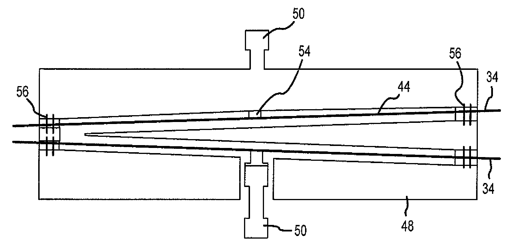
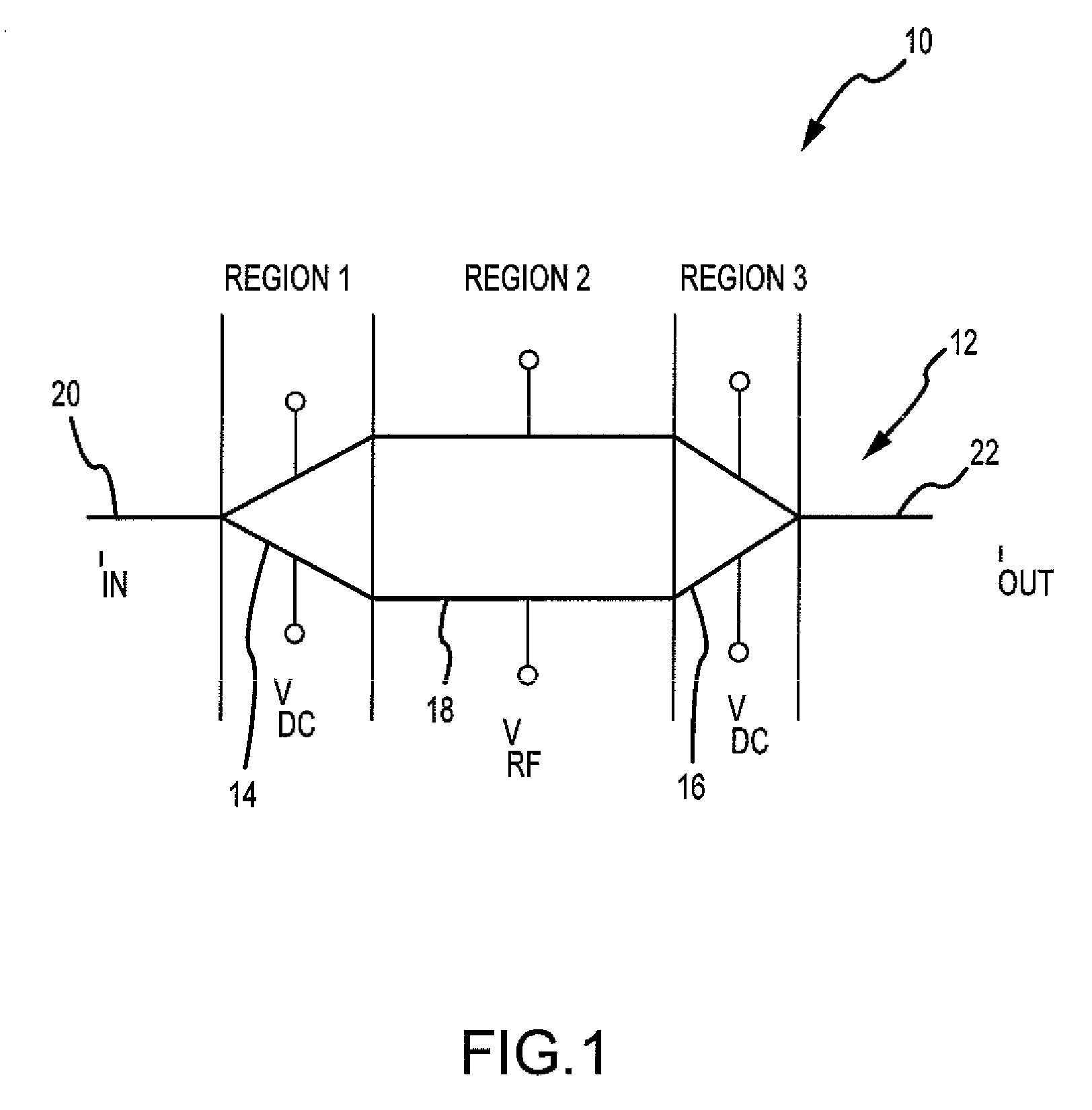
[0021]Disclosed embodiments will now be described more fully hereinafter with reference to the accompanying drawings, in which some, but not all disclosed embodiments are shown. Indeed, several different embodiments may be provided and should not be construed as limited to the embodiments set forth herein. Rather, these embodiments are provided so that this disclosure will be thorough and complete and will fully convey the scope of the disclosure to those skilled in the art.

[0022]The device and method of the disclosed embodiments may be used in connection with various applications including, but not limited to, long distance communication systems, such as free space laser communication systems for satellite and terrestrial applications, and terrestrial and underwater fiber optic communication systems. Accordingly, one of ordinary skill in the art will recognize and appreciate that the device and method of the disclosure can be used in any number of applications involving LN electro-...


PUM

PropertyMeasurementUnit
thicknessaaaaaaaaaa
refractive indexaaaaaaaaaa

Abstract

There is provided in one of the embodiments of the disclosure a lithium niobate modulator structure for mitigating DC bias drift comprising a highly doped semiconductor layer patterned above an optical waveguide having one or more DC sections and an RF section, wherein a metal layer or contact is in contact with a portion of the semiconductor layer and a buffer layer is deposited in the RF section. There is provided in another embodiment of the disclosure a method for making a lithium niobate electro-optical modulator for mitigation of DC bias drift.

Description

BACKGROUND OF THE DISCLOSURE[0001]1) Field of the Disclosure[0002]The disclosure relates to lithium niobate electro-optical modulators, and more particularly, to a lithium niobate electro-optical modulator having a doped semiconductor structure for the mitigation of DC bias drift.[0003]2) Description of Related Art[0004]Electro-optical modulators are optical devices in which a signal-controlled element displaying electro-optic effect is used to modulate a beam of light. Electro-optical modulators are key components for high-speed optical transmission systems. Such electro-optical modulators are typically made from lithium niobate (LiNbO3), referred to as “LN”, because of its high electro-optic coefficient and high-quality crystals. LN modulators are primarily used as electro-optical modulators that convert high-speed electrical signals to optical signals for long distance communication systems, such as free space laser communication systems for satellite and terrestrial applications...

Claims


Application Information

Patent Timeline
Patent Type & Authority Applications(United States)
IPC IPC(8): G02F1/035H01L21/02
CPCG02F1/0316G02F1/2255G02F2203/21G02F2202/10G02F2201/07G02F1/03G02F1/225
Inventor SAYYAH, KEYVANHAYES, ROBERT R.
Owner THE BOEING CO
Why Eureka
Try Eureka