

Method for projecting wafer product overlay error and wafer product critical dimension
a technology of product overlay and critical dimension, which is applied in the direction of semiconductor/solid-state device testing/measurement, instruments, photomechanical apparatus, etc., can solve the problem that the measuring instrument cannot find bad wafer products, and achieve the effect of improving the efficiency of manufacturing wafer products
- Summary
- Abstract
- Description
- Claims
- Application Information
AI Technical Summary
Benefits of technology
Problems solved by technology
Method used
Image

Examples
Embodiment Construction
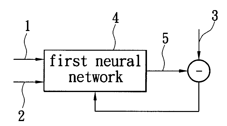
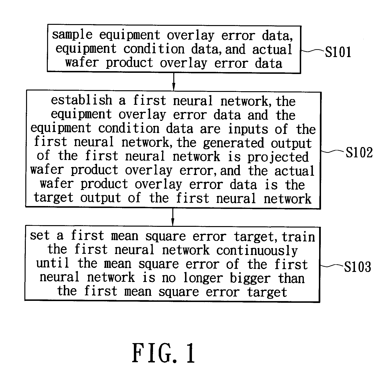
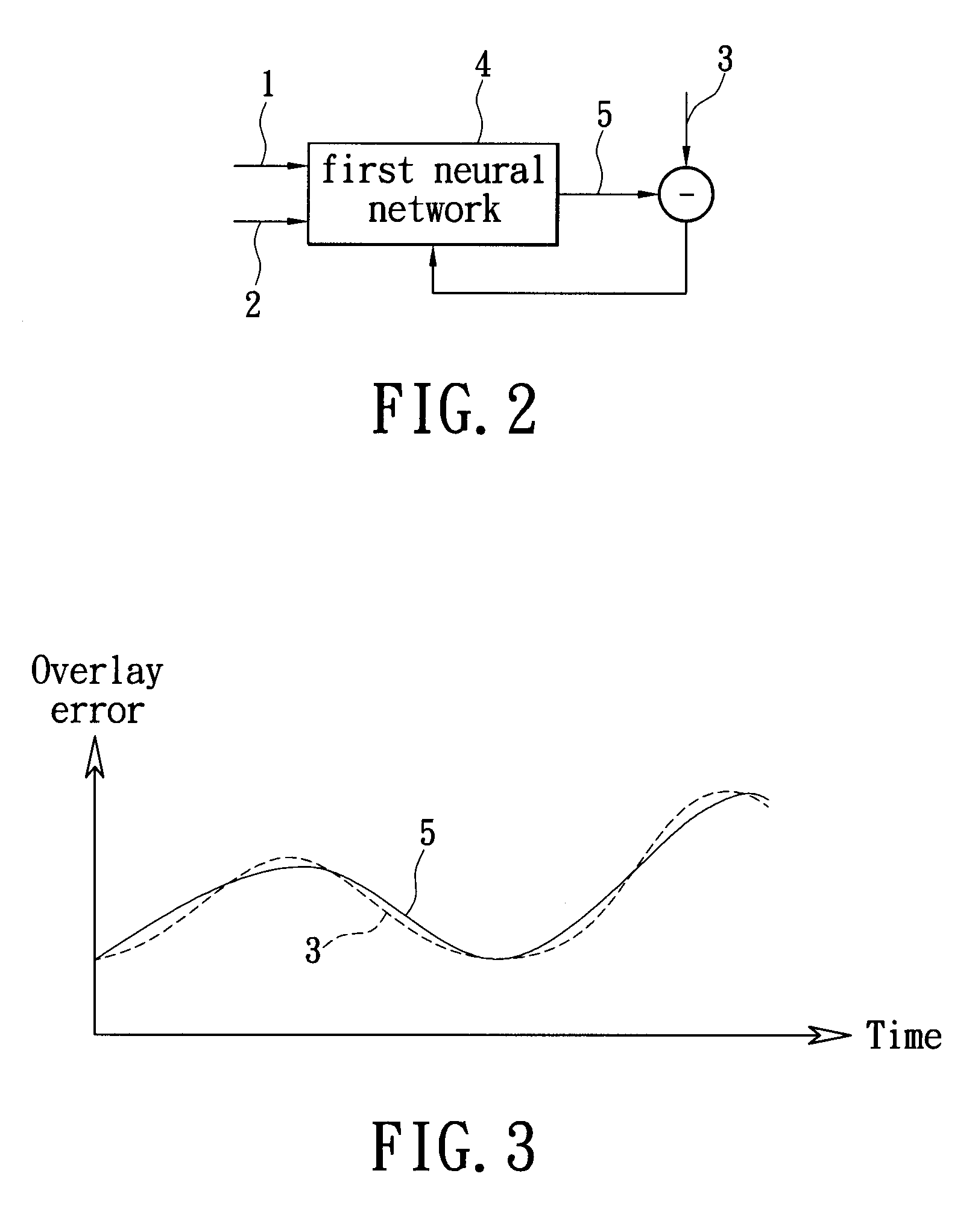
[0026]As shown in FIGS. 1 and 2, a method for projecting wafer product overlay error is presented, and the steps of the method comprise:
[0027]S101: sample equipment overlay error data 1, equipment condition data 2, and actual wafer product overlay error data 3, wherein the equipment overlay error data 1 indicates manufacturing ability of manufacturing machines, if a batch of wafers which is transported to the manufacturing machine whose manufacturing ability is better, the overlay error of the batch of wafer product is smaller;
[0028]S102: establish a first neural network 4, the first neural network 4 can be chosen as a back-propagation neural network, the equipment overlay error data 1 and the equipment condition data 2 are inputs of the first neural network 4, the generated output of the first neural network 4 is projected wafer product overlay error 5, and the actual wafer product overlay error data 3 is the target output of the first neural network 4. Therein the actual wafer pro...
PUM
 Abstract
Description
Claims
Application Information