Error control in a flash memory device
a flash memory device and error control technology, applied in the field of flash memory devices, can solve the problem and achieve the effect of greater average storage capacity of flash memory cells over tim
- Summary
- Abstract
- Description
- Claims
- Application Information
AI Technical Summary
Benefits of technology
Problems solved by technology
Method used
Image
Examples
Embodiment Construction
[0025]FIGS. 1-6 and the following description depict specific exemplary embodiments of the invention to teach those skilled in the art how to make and use the invention. For the purpose of teaching inventive principles, some conventional aspects of the invention have been simplified or omitted. Those skilled in the art will appreciate variations from these embodiments that fall within the scope of the invention. Those skilled in the art will appreciate that the features described below can be combined in various ways to form multiple variations of the invention. As a result, the invention is not limited to the specific embodiments described below, but only by the claims and their equivalents.
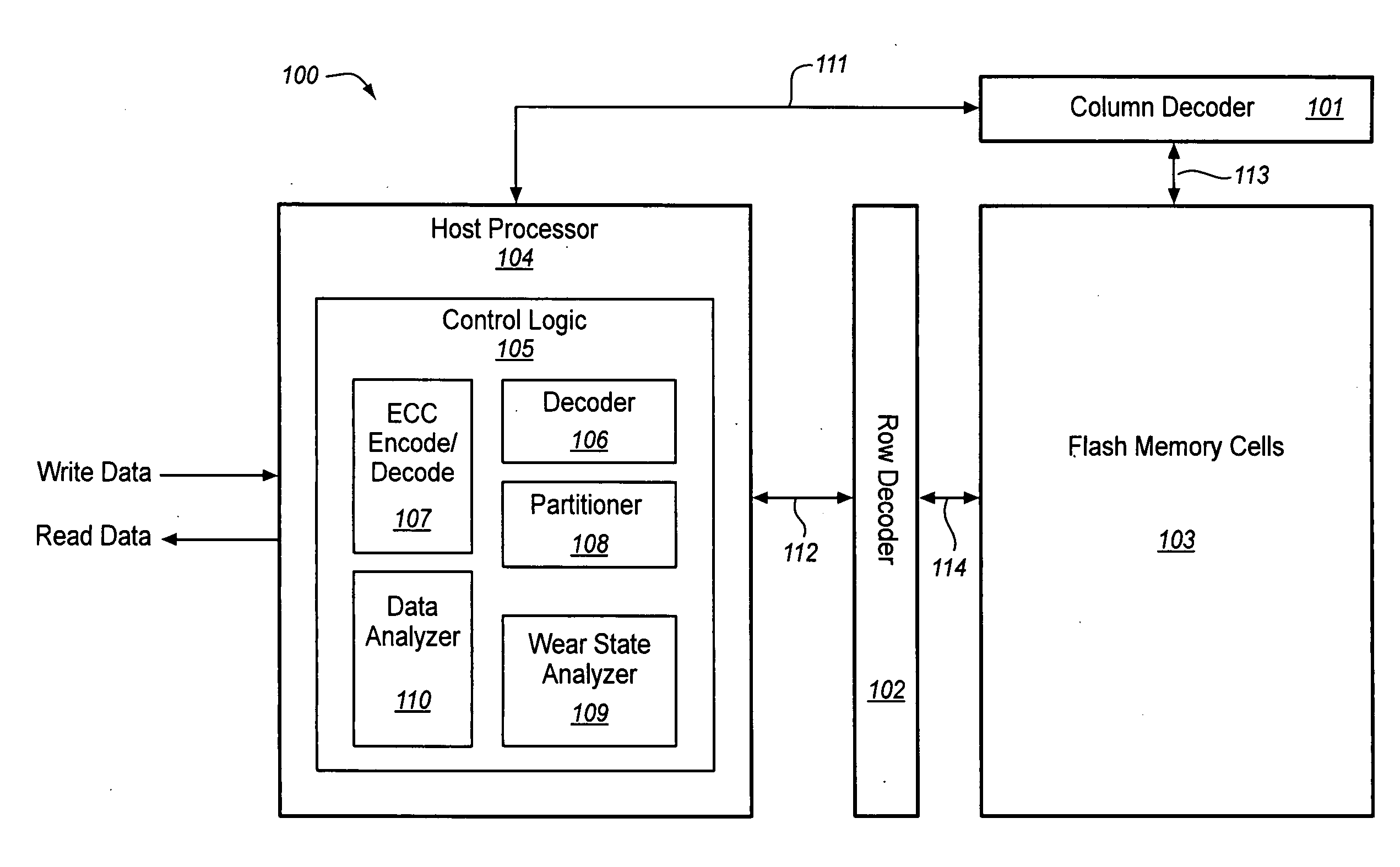
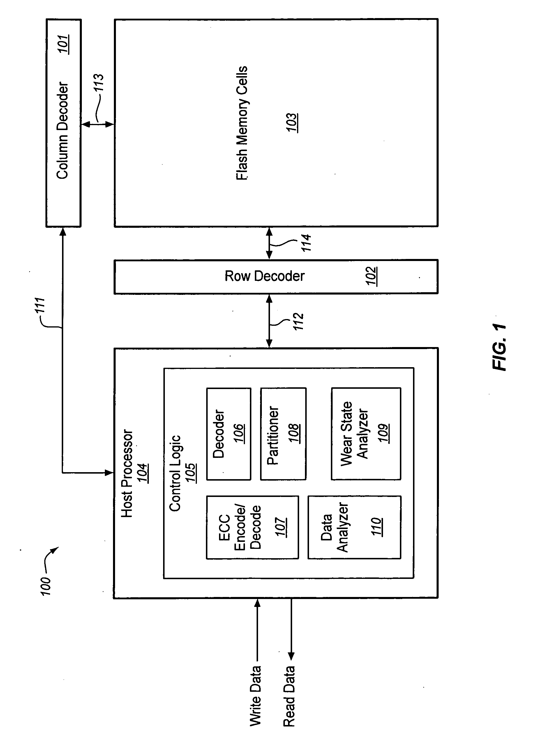
[0026]FIG. 1 shows a block diagram of flash memory device 100 including an array of flash memory cells 103. Flash memory device 100 also includes host processor 104 that provides for general control of flash memory device 100. Flash memory cells 103 are individually addressable and arranged in t...
PUM
 Abstract
Description
Claims
Application Information


