
Semiconductor device having vertical field effect transistor and method of manufacturing the same

Inactive Publication Date: 2010-03-04
RENESAS ELECTRONICS CORP
View PDF18 Cites 15 Cited by
  • Summary
  • Abstract
  • Description
  • Claims
  • Application Information

AI Technical Summary

Benefits of technology

[0021]According to the present invention, it is possible to further improve the integration in the semiconductor device using the vertical field effect transistor.

Problems solved by technology

However, further miniaturization of a typical MISFET is becoming more difficult, because it causes problems such as increase in leakage current and characteristics variability.
That is, it is becoming more difficult to further improve the integration with using a typical MISFET.
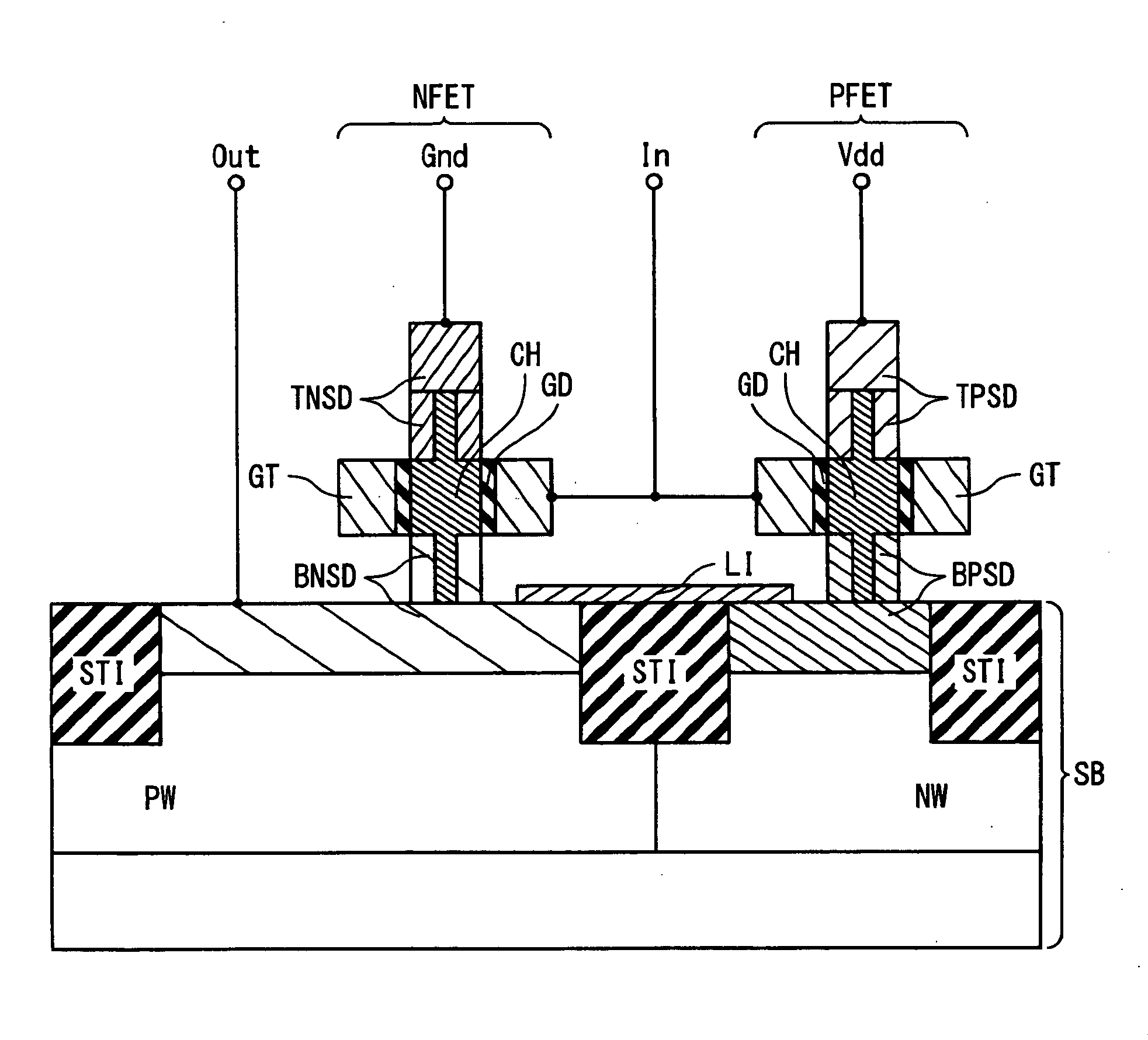
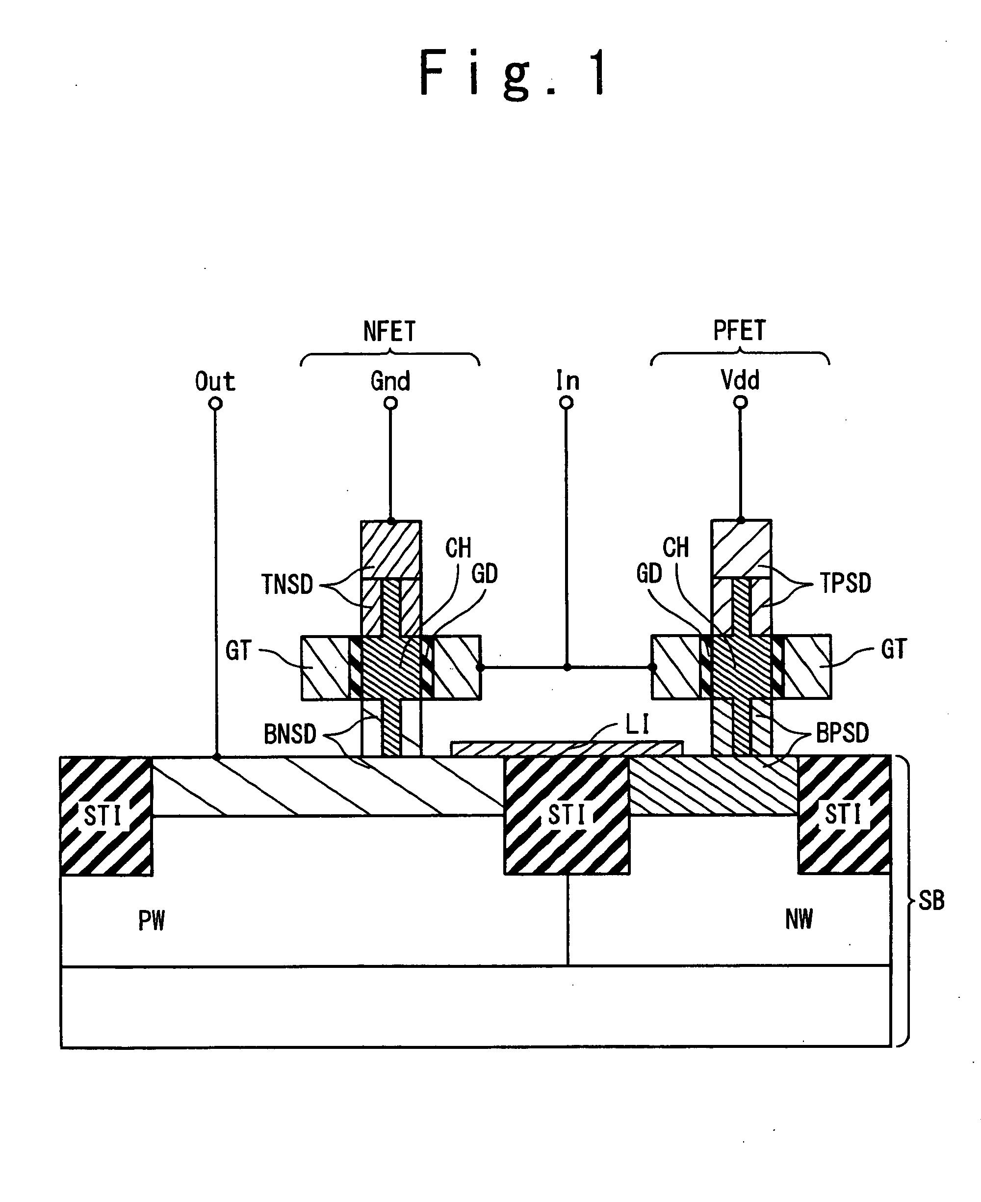
That is to say, the NFET and the PFET need to be separated by the device isolation structure STI, and thus it is not possible to make the NFET and the PFET closer to each other.
This interferes improvement in the integration.
However, to secure a sufficient contact area between the source / drain sections (BNSD, BPSD) and the local metal wiring LI causes increase in a circuit area and hence deterioration in the integration.

Method used


Image

  • Semiconductor device having vertical field effect transistor and method of manufacturing the same
  • Semiconductor device having vertical field effect transistor and method of manufacturing the same
  • Semiconductor device having vertical field effect transistor and method of manufacturing the same

Examples


modification example

4. MODIFICATION EXAMPLE

4-1. First Modification Example

[0089]The pattern of the openings R1 and R2 of the alloying inhibition film 30 in FIG. 5D is not limited to that shown in FIG. 6. The pattern of the openings R1 and R2 of the alloying inhibition film 30 can be that shown in FIG. 7. In the example shown in FIG. 7, a part of the pattern of the openings R1 and R2 protrudes from a region where the semiconductor layers 21 and 22 are formed. In this case, at least a part of the sides of the formed metal layers 51 and 52 is defined in a self-aligned manner by the boundary of the semiconductor layers 21 and 22 as a base layer. Therefore, even if displacement of the openings R1 and R2 occurs, variability of shapes of the formed metal layers 51 and 52 can be suppressed. In the case where the openings R1 and R2 shown in FIG. 7 are used, a cross-sectional shape shown in FIG. 8 is obtained instead of that shown in the foregoing FIG. 5F. It should be noted that the right-side boundary of the s...

second modification example

4-2. Second Modification Example

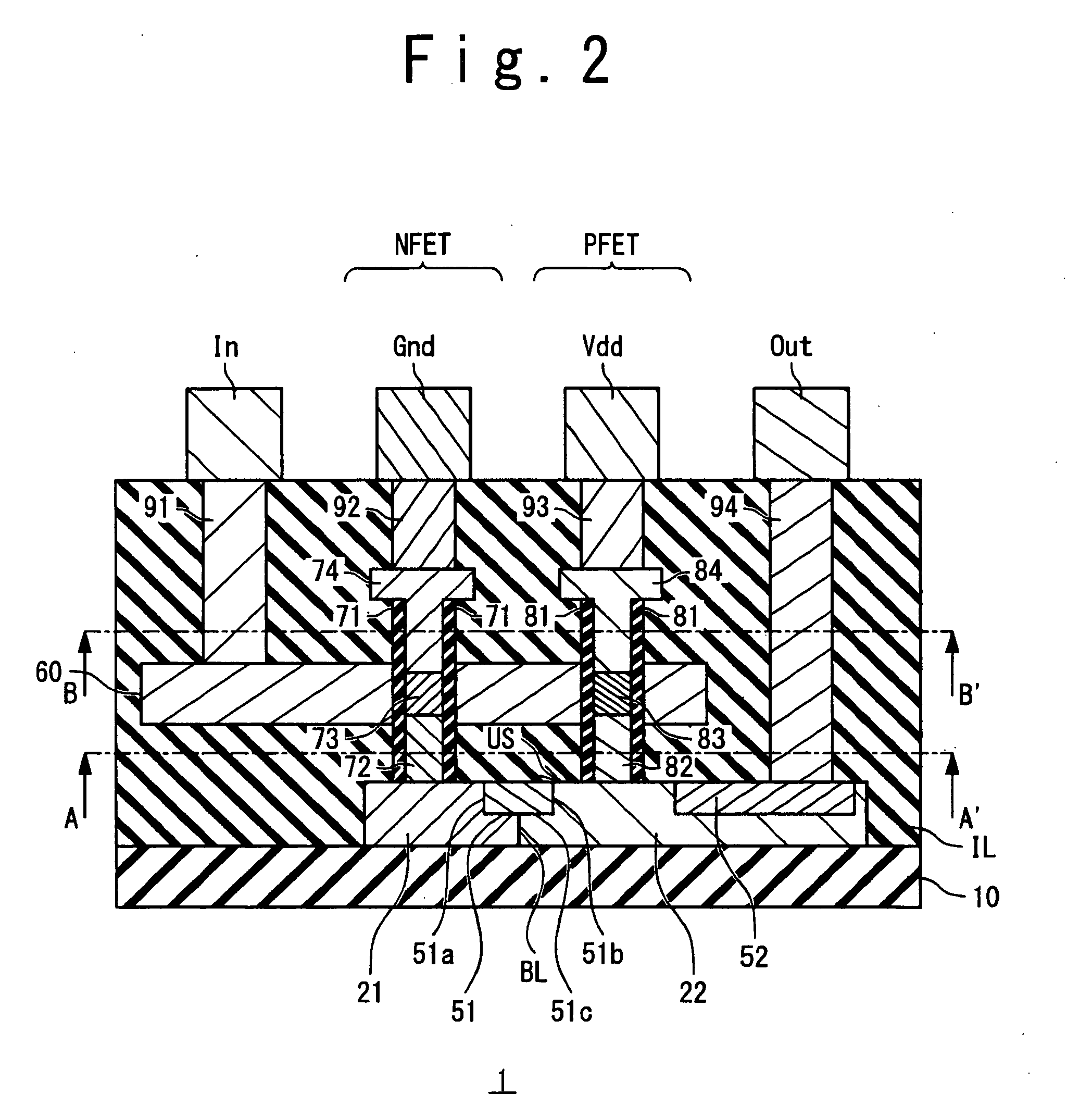
[0090]In the actual manufacturing process, the cross-sectional shape of the metal layers 51 and 52 can be rounded shape as shown in FIG. 9 instead of strict rectangle. Even in this case, the fact remains that the first metal layer 51 is formed to be embedded in the N-type semiconductor layer 21 and the P-type semiconductor layer 22. That is, the first metal layer 51 has the first side surface 51a being in contact with the N-type semiconductor layer 21, the second side surface 51b being in contact with the P-type semiconductor layer 22, and the bottom surface 51c being in contact with both of the N-type semiconductor layer 21 and the P-type semiconductor layer 22. In order to significantly reduce the contact resistance, a buried depth LD of the first metal layer 51 is more than 5% (preferably 10%) of a width LW of the first metal layer 51. The same applies to the second metal layer 52.

[0091]Moreover, it is not necessary that upper surfaces of the metal...

third modification example

4-3. Third Modification Example

[0092]As shown in FIG. 10, the metal layers 51 and 52 may be formed to be in contact with the insulating substrate 10. In this case, the first metal layer 51 lies between the N-type semiconductor layer 21 and the P-type semiconductor layer 22. That is to say, the N-type semiconductor layer 21 and the P-type semiconductor layer 22 are electrically connected with each other through the first metal layer 51. Also in this case, there is no need to form a device isolation structure between the N-type semiconductor layer 21 and the P-type semiconductor layer 22. The N-type semiconductor layer 21 and the P-type semiconductor layer 22 are short-circuited to each other without through a device isolation structure. Therefore, the integration is improved.

[0093]In the case of the example shown in FIG. 10, the bottom surface 51c of the first metal layer 51 is in contact with the insulating substrate 10. That is, the bottom surface 51c of the first metal layer 51 is...


PUM


Abstract

A semiconductor device has: an insulating substrate; a first semiconductor layer of a first conductivity type formed on the insulating substrate; a first vertical field effect transistor of the first conductivity type, one of whose source and drain being formed on the first semiconductor layer; a second semiconductor layer of a second conductivity type formed on the insulating substrate; and a second vertical field effect transistor of the second conductivity type, one of whose source and drain being formed on the second semiconductor layer. The first semiconductor layer and the second semiconductor layer are directly in contact with each other.

Description

INCORPORATION BY REFERENCE[0001]This application is based upon and claims the benefit of priority from Japanese patent application No. 2008-218155, filed on Aug. 27, 2008, the disclosure of which is incorporated herein in its entirety by reference.BACKGROUND OF THE INVENTION[0002]1. Field of the Invention[0003]The present invention relates to a semiconductor device. In particular, the present invention relates to a semiconductor device having a vertical field effect transistor and a method of manufacturing the same.[0004]2. Description of Related Art[0005]A MISFET (Metal Insulator Semiconductor Field Effect Transistor) has been miniaturized, which achieves improvement in integration and performance. In recent years, the MISFET reaches a level where a thickness of its gate insulating film is less than 2 nm and its gate length is less than 50 nm. However, further miniaturization of a typical MISFET is becoming more difficult, because it causes problems such as increase in leakage curr...

Claims


Application Information

Patent Timeline
IPC IPC(8): H01L27/092
CPCH01L21/823487H01L21/84H01L27/092H01L29/78642H01L29/41733H01L29/42392H01L27/1203H01L29/7827
Inventor TAKEUCHI, KIYOSHI
Owner RENESAS ELECTRONICS CORP
Learn More