A sealing structure and method of manufacturing the same

Active Publication Date: 2010-03-04
NXP BV
View PDF10 Cites 8 Cited by
  • Summary
  • Abstract
  • Description
  • Claims
  • Application Information

AI Technical Summary

Benefits of technology

[0006]It is an object of the invention to provide

Problems solved by technology

However, the procedure of forming polysilicon sealed vacuum ca

Method used


Image

  • A sealing structure and method of manufacturing the same
  • A sealing structure and method of manufacturing the same
  • A sealing structure and method of manufacturing the same

Examples


Embodiment Construction

[0059]The illustration in the drawing is schematical. In different drawings, similar or identical elements are provided with the same reference signs.

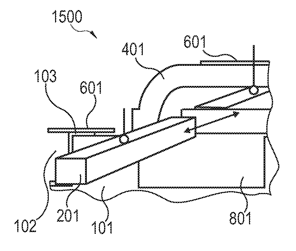
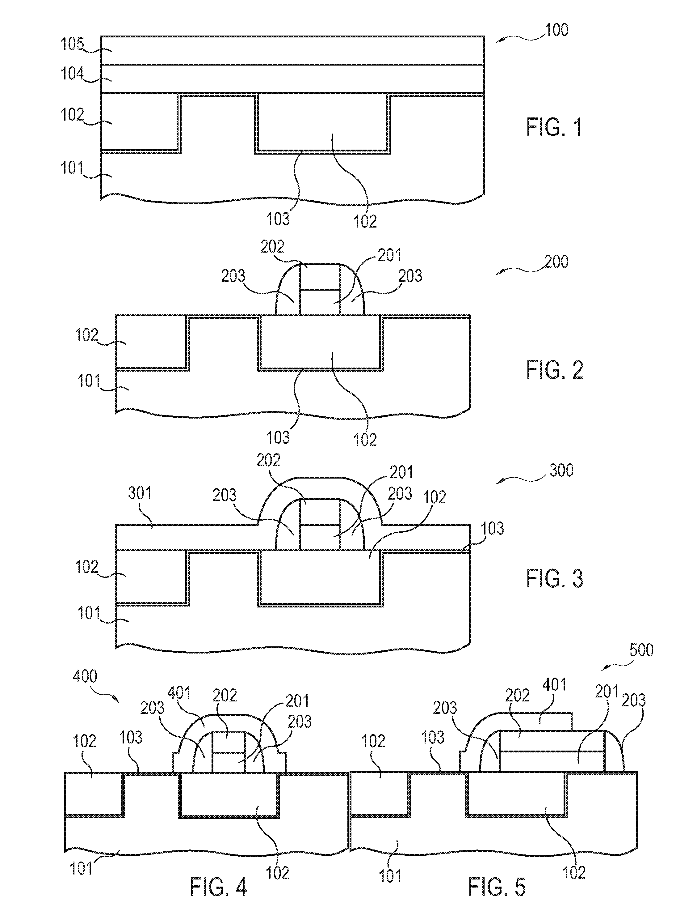
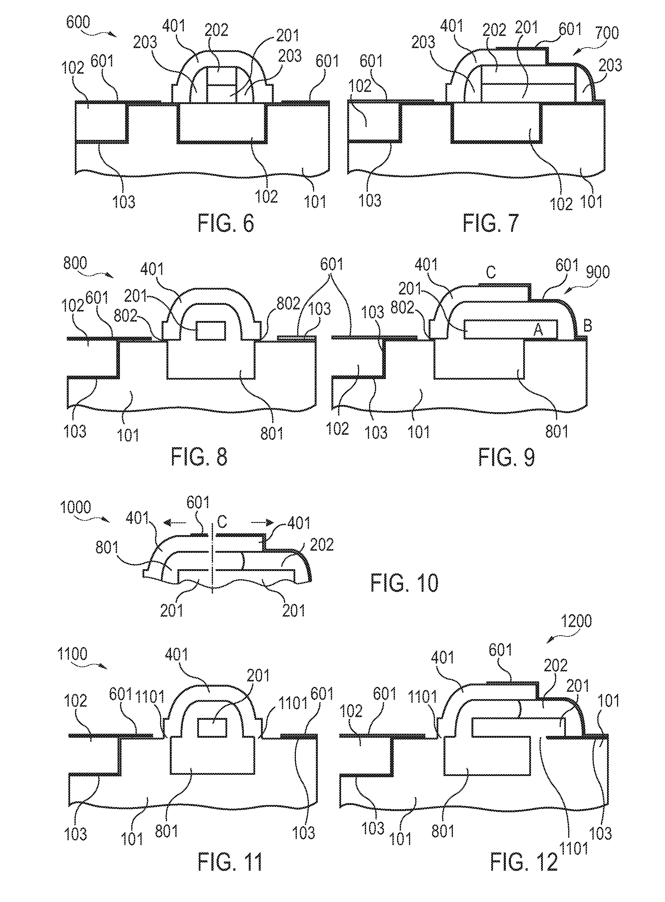
[0060]In the following, referring to FIG. 1 to FIG. 15, a method of forming a MEMS resonator structure 1100 according to an exemplary embodiment of the invention will be explained. More particularly, a detailed process flow for a MEMS resonator is shown.

[0061]As shown in FIG. 1, starting point is an STI (Shallow Trench Insulation) patterned wafer 101 with the pre-gate oxide on active.

[0062]More particularly, FIG. 1 shows a crystalline silicon wafer 101 having a thermally grown silicon oxide layer 103 as a first sacrificial layer and having, deposited in trenches of the silicon substrate 101, silicon oxide portions 102 as second sacrificial structures. On top of the structure 100, a polysilicon layer 104 is formed which may later serve as a basis for a MEMS resonator. On top of the polysilicon layer 104, a TEOS layer 105 (tetraethylorth...


PUM


Abstract

A method of manufacturing a structure (1100), the method comprising forming a cap element (401) on a substrate (101), removing material (103) of the substrate (101) below the cap element (401) to thereby form a gap (802) between the cap element (401) and the substrate (101), and rearranging material of the cap element (401) and/or of the substrate (101) to thereby merge the cap element (401) and the substrate (101) to bridge the gap (802).

Description

FIELD OF THE INVENTION[0001]The invention relates to a method of manufacturing a structure.[0002]Moreover, the invention relates to a structure.BACKGROUND OF THE INVENTION[0003]The technology of MEMS (micro-electro-mechanical systems) is related to devices comprising an electronic part which may be fabricated using integrated circuit (IC) process sequences, and comprises a micromechanical component which is usually fabricated using compatible “micromachining” processes that selectively remove (for instance etch away) parts of a semiconductor (for instance silicon) wafer and / or that add new structured layers to form the mechanical and electromechanical devices.[0004]Zook, J D, Herb, W R, Ahn, Y and Guckel, H, “Polysilicon sealed vacuum cavities for microelectromechanical systems”, J. Vac. Sci. Technol. A 17(4), July / August 1999 discloses sealed vacuum cavities used in silicon-based micro-electro-mechanical systems. Sealed polysilicon cavities may serve as reference chambers for press...

Claims


Application Information

Patent Timeline
IPC IPC(8): H01L29/84H01L21/306
CPCB81B2201/0271B81C2203/0145B81C1/00293
Inventor DONKERS, JOHANNESHIJZEN, ERWINMEUNIER-BEILLARD, PHILIPPEKOOPS, GERHARD
Owner NXP BV
Why Eureka
Try Eureka