Substrate for semiconductor package and semiconductor package having the same

Active Publication Date: 2010-03-04
SK HYNIX INC
View PDF3 Cites 16 Cited by
  • Summary
  • Abstract
  • Description
  • Claims
  • Application Information

AI Technical Summary

Benefits of technology

[0006]Embodiments of the present invention are directed to a substrate for a semiconductor package which reduces the diffe

Problems solved by technology

When semiconductor packages are stacked into a single semiconductor package unit, problems hindering high-speed operations could arise in the single semiconductor pa

Method used


Image

  • Substrate for semiconductor package and semiconductor package having the same
  • Substrate for semiconductor package and semiconductor package having the same
  • Substrate for semiconductor package and semiconductor package having the same

Examples


Example

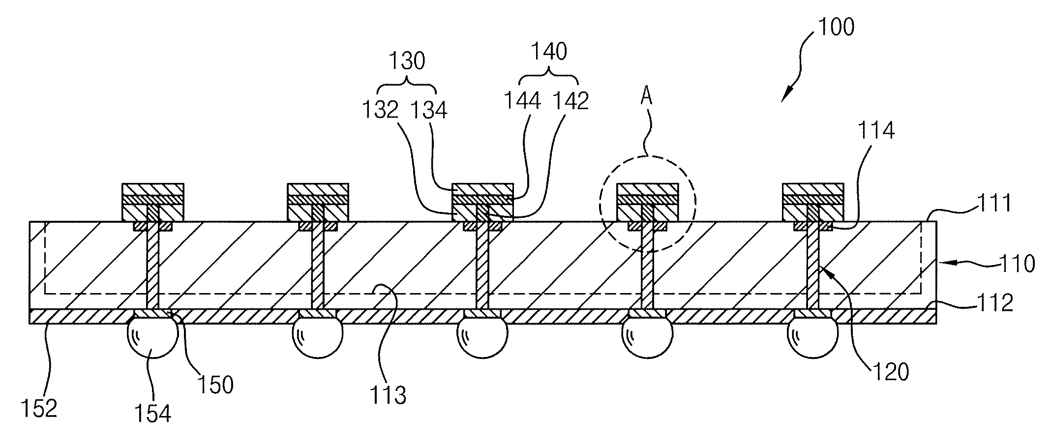
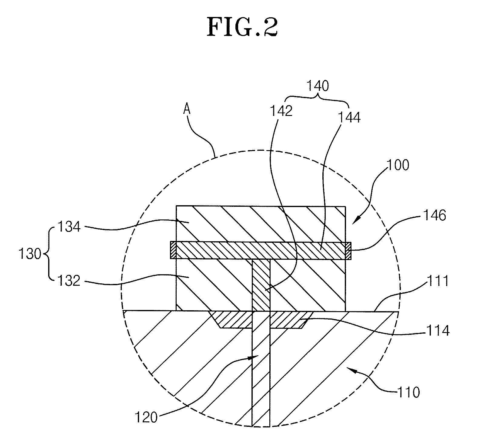
[0028]FIG. 1 is a cross-sectional view showing a substrate 100 for a semiconductor package in accordance with an embodiment of the present invention. FIG. 2 is an enlarged view of a portion ‘A’ of the substrate 100 shown in FIG. 1.

[0029]Referring to FIGS. 1 and 2, the substrate 100 for a semiconductor package includes a substrate body 110, a through electrode 120, an insulation member 130, and a connection member 140.

[0030]The substrate body 110 is a planar layer (for example, a plate shape with a rectangular parallelepiped shape) having a first face 111 and a second face 112 opposing the first face 111.

[0031]In the present embodiment, the substrate body 110 is a semiconductor chip having a circuit unit 113 and bonding pads 114.

[0032]The circuit unit 113 may include a data storing unit (not shown) for storing data and / or a data processing unit (not shown) for processing the data. The bonding pads 114 may be disposed, for example, on the first face 111 of the substrate body 110, and ...


PUM


Abstract

A semiconductor package includes a substrate including a substrate body having a first face and a second face opposing the first face. A first through electrode passes through the substrate body between the first face and the second face. An insulation member is disposed over the first face; and a connection member having a first conductive unit disposed inside of the insulation member is electrically connected to the first through electrode, and 10 a second conductive unit electrically connected to the first conductive unit is exposed at side faces of the insulation member. A semiconductor chip having third and fourth faces is disposed over the first face of the substrate body in a vertical direction. A second through electrode passes through the substrate body between the third and fourth faces and is electrically connected to the second conductive unit.

Description

CROSS-REFERENCE TO RELATED APPLICATIONS[0001]The present application claims priority to Korean patent application number 10-2008-0085389 filed on Aug. 29, 2008, which is incorporated herein by reference in its entirety.BACKGROUND OF THE INVENTION[0002]The present invention relates generally to semiconductor packages, and more particularly to a substrate for a semiconductor package and a semiconductor package having the same.[0003]Nowadays, semiconductor chips capable of storing massive data in a short processing time and semiconductor packages having such semiconductor chips packaged therein are being developed.[0004]To enhance the data storing capacity and / or the data processing speed of a semiconductor package, a semiconductor package having a plurality of electrically interconnected semiconductor packages stacked on a substrate is also being developed.[0005]When semiconductor packages are stacked into a single semiconductor package unit, problems hindering high-speed operations c...

Claims


Application Information

Patent Timeline
IPC IPC(8): H01L29/40H01L23/52
CPCH01L23/481H05K2201/10674H01L23/49827H01L24/13H01L24/29H01L24/32H01L25/0657H01L2224/13021H01L2225/06541H01L2225/06551H01L2225/06572H01L2924/01078H01L2924/078H01L2924/15311H01L2924/19042H01L2924/19043H05K1/183H05K1/184H05K2201/092H01L23/49811H01L2224/05573H01L2224/13025H01L2224/05647H01L2924/00014H01L2224/0554H01L2224/16145H01L2224/16146H01L2224/16105H01L2224/16106H01L2224/13076H01L2224/131H01L2224/13564H01L2224/1357H01L2224/136H01L2224/81192H01L24/05H01L2224/05599H01L2224/0555H01L2224/0556H01L2924/014H01L23/48
Inventor SUH, MIN SUK
Owner SK HYNIX INC
Why Eureka
Try Eureka