Method for manufacturing flash memory device

Active Publication Date: 2005-04-26
MICRON TECH INC
View PDF3 Cites 14 Cited by
  • Summary
  • Abstract
  • Description
  • Claims
  • Application Information

AI Technical Summary

Benefits of technology

[0008]Accordingly, the present invention is directed to provide a method of manufacturing a flash memory device capable of reducing a difference in effective field oxide heights between a high voltage t

Problems solved by technology

Such a difference in EFH's between the high voltage transistor area HV and the low voltage transistor/cell area LV/CELL and the high value of EFH's in the low voltage transistor/cell area LV/CE

Method used


Image

  • Method for manufacturing flash memory device
  • Method for manufacturing flash memory device
  • Method for manufacturing flash memory device

Examples


Embodiment Construction

[0015]The present invention will be described in detail by way of the preferred embodiment with reference to the accompanying drawings, in which like reference numerals are used to identify the same or similar parts.

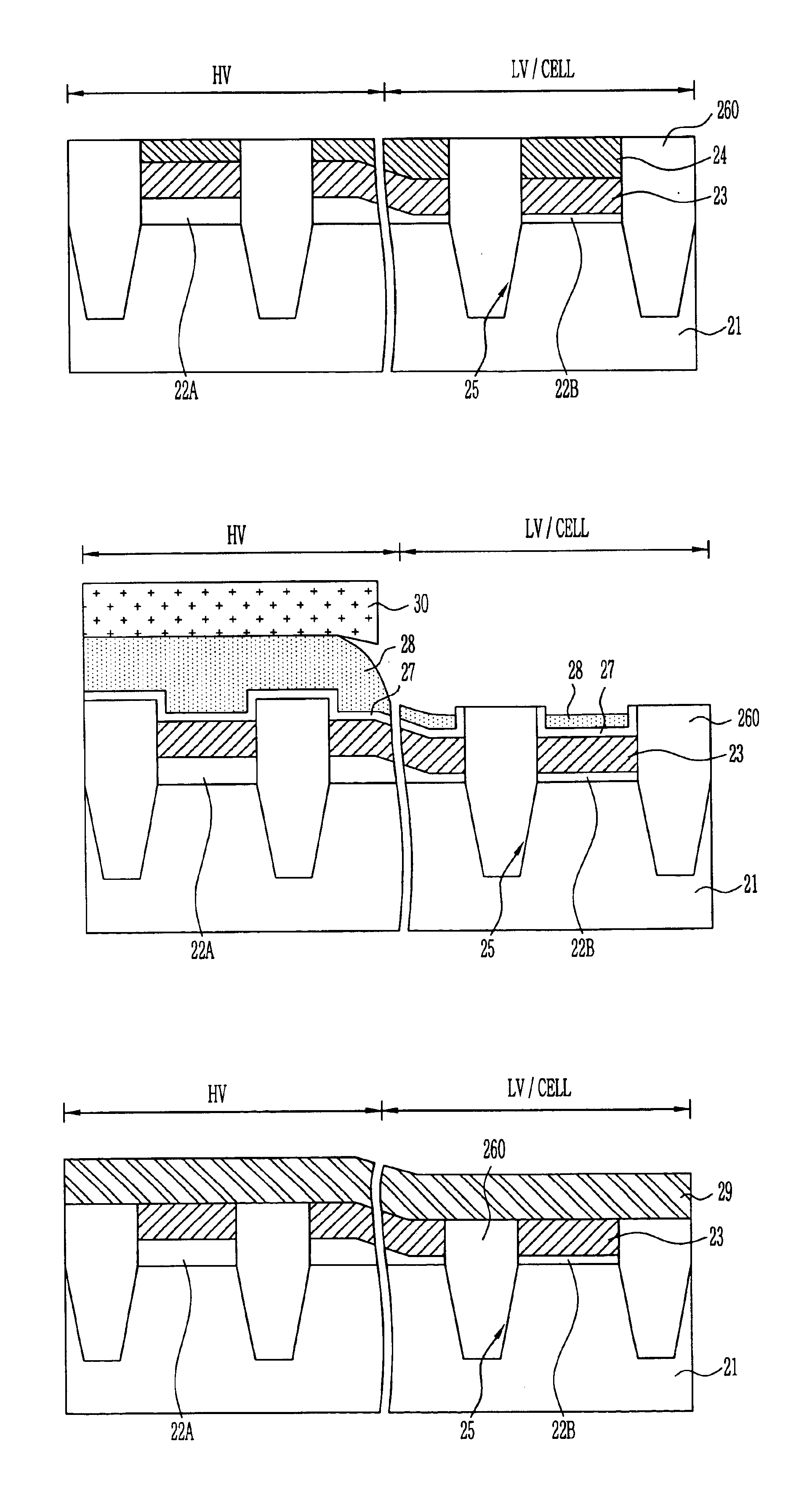
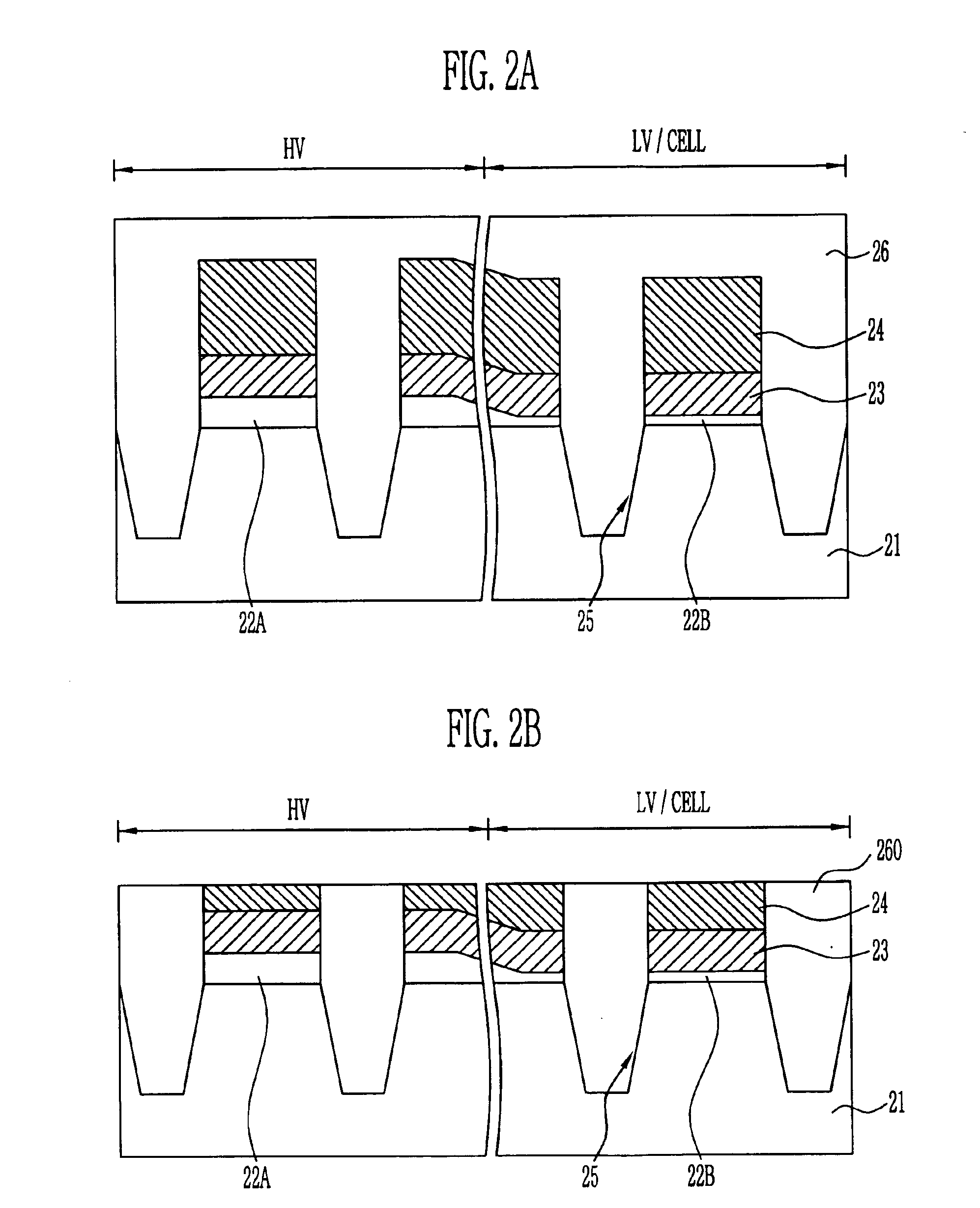
[0016]Shown in FIGS. 2A to 2F are cross-sectional views for illustrating a method of manufacturing a flash memory device formed by applying a SA-STI scheme according to an embodiment of the present invention.

[0017]Although a flash memory device includes a cell area, a low voltage transistor area, and a high voltage transistor area—the cell area and the low voltage transistor area will be considered as one area—the low voltage transistor / cell area—in the following description for easier understanding because the thickness of their gate oxides is similar to each other.

[0018]Referring to FIG. 2A, a gate oxide film 22A for a high voltage is formed on a semiconductor substrate 21 in the high voltage transistor area HV, and a gate oxide film 22B for a low voltage / cell is forme...


PUM


Abstract

The present invention relates to a method of manufacturing a flash memory device. In a flash memory device formed by applying a self-align shallow trench isolation (SA-STI) scheme, a polishing process and a process for removing a nitride film are performed after oxide materials are buried in isolation trenches. Then, oxide films with an excellent planarization are formed, a first etching process is performed to selectively remove the oxide films in a low voltage transistor/cell area to a certain thickness, a second etching process is performed to remove the oxide films in a high voltage transistor area and the low voltage transistor/cell area until a poly-silicon layer for a floating gate is exposed. Therefore, protruding portions of element isolation films in the high voltage transistor area and the low voltage transistor/cell area are etched away to a certain thickness during the first and second etching processes so that a difference in EFH's between these areas can be reduced.

Description

BACKGROUND[0001]1. Field of the Invention[0002]The present invention relates to a method of manufacturing a flash memory device, and more particularly to a method of manufacturing a flash memory device capable of reducing a difference in effective field oxide heights (“EFH”) between a high voltage transistor area, and a low voltage transistor / cell area, which is caused by respective protruding portions of element isolation films thereon in a flash memory device manufactured by applying a self-align shallow trench isolation (“SA-STI”) scheme.[0003]2. Discussion of Related Art[0004]Basically, a flash memory device has low voltage transistors and high voltage transistors in order to drive cells according to necessary properties. Usually, a gate oxide film for the high voltage transistor is made to be thick, on the other hand, in case of the low voltage transistor, it is made to be thin. The thickness of a gate oxide film for a cell is equal or similar to that for a low voltage transist...

Claims


Application Information

Patent Timeline
IPC IPC(8): H01L21/762H01L21/70H01L21/8234H01L21/8247H01L27/105H01L27/10H01L27/115H01L29/788H01L29/792
CPCH01L21/76224H01L21/823462H01L27/11541H01L27/105H01L27/11526H01L21/823481H10B41/40H10B41/47H10B69/00
Inventor LEE, BYOUNG KI
Owner MICRON TECH INC
Why Eureka
Try Eureka