Fabrication method of a flash memory device

Inactive Publication Date: 2005-02-15
POWERCHIP SEMICON MFG CORP
View PDF1 Cites 8 Cited by
  • Summary
  • Abstract
  • Description
  • Claims
  • Application Information

AI Technical Summary

Benefits of technology

Accordingly, the present invention provides a structure of a flash memory device and a fabrication method for the same, wherein forming an additional source line pickup is obviated wh

Problems solved by technology

Further, an ineffective isolation between the bit lines is resulted.
Further, the diffusion of the P-well driving-in is difficult to control.
The efficiency and the yield of the device are adversely affected.
Since the resistance of a deep N-type well region is higher, the operational speed is affected.
However, forming a sou

Method used


Image

  • Fabrication method of a flash memory device
  • Fabrication method of a flash memory device
  • Fabrication method of a flash memory device

Examples


Embodiment Construction

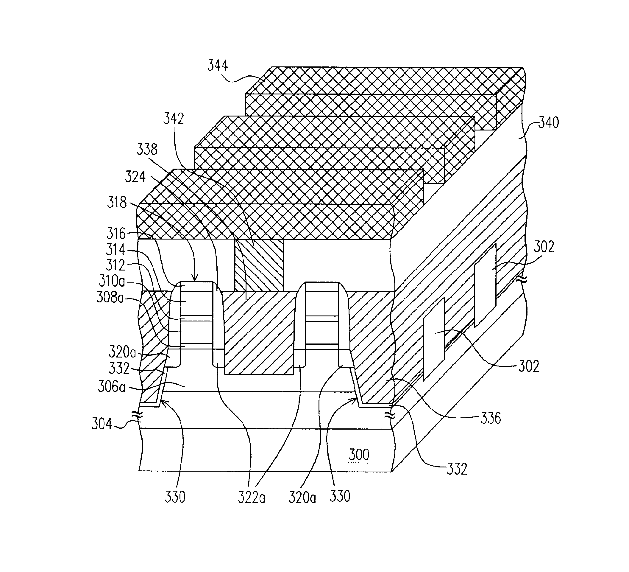
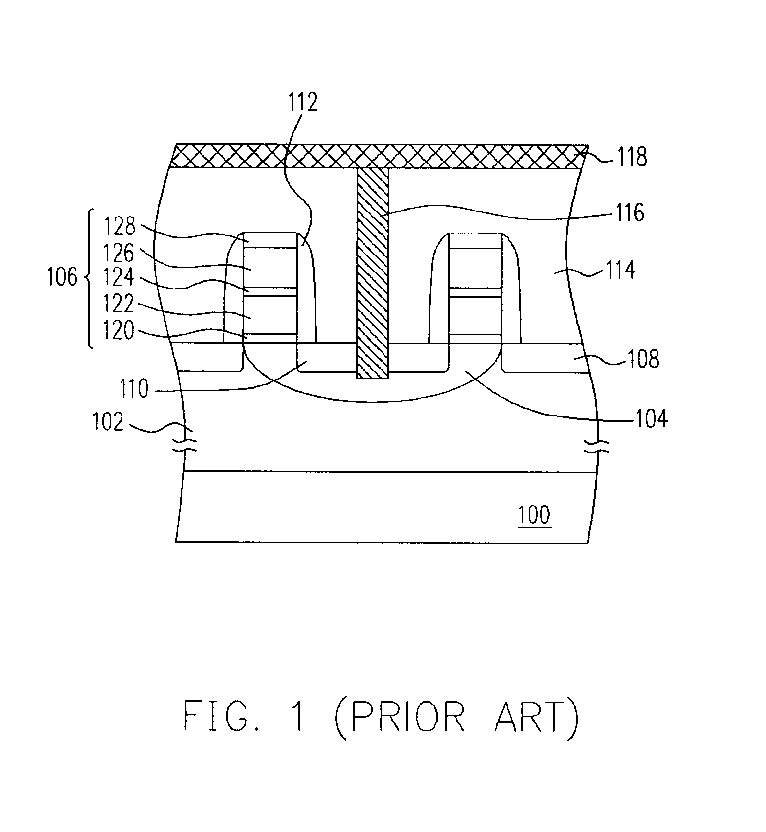
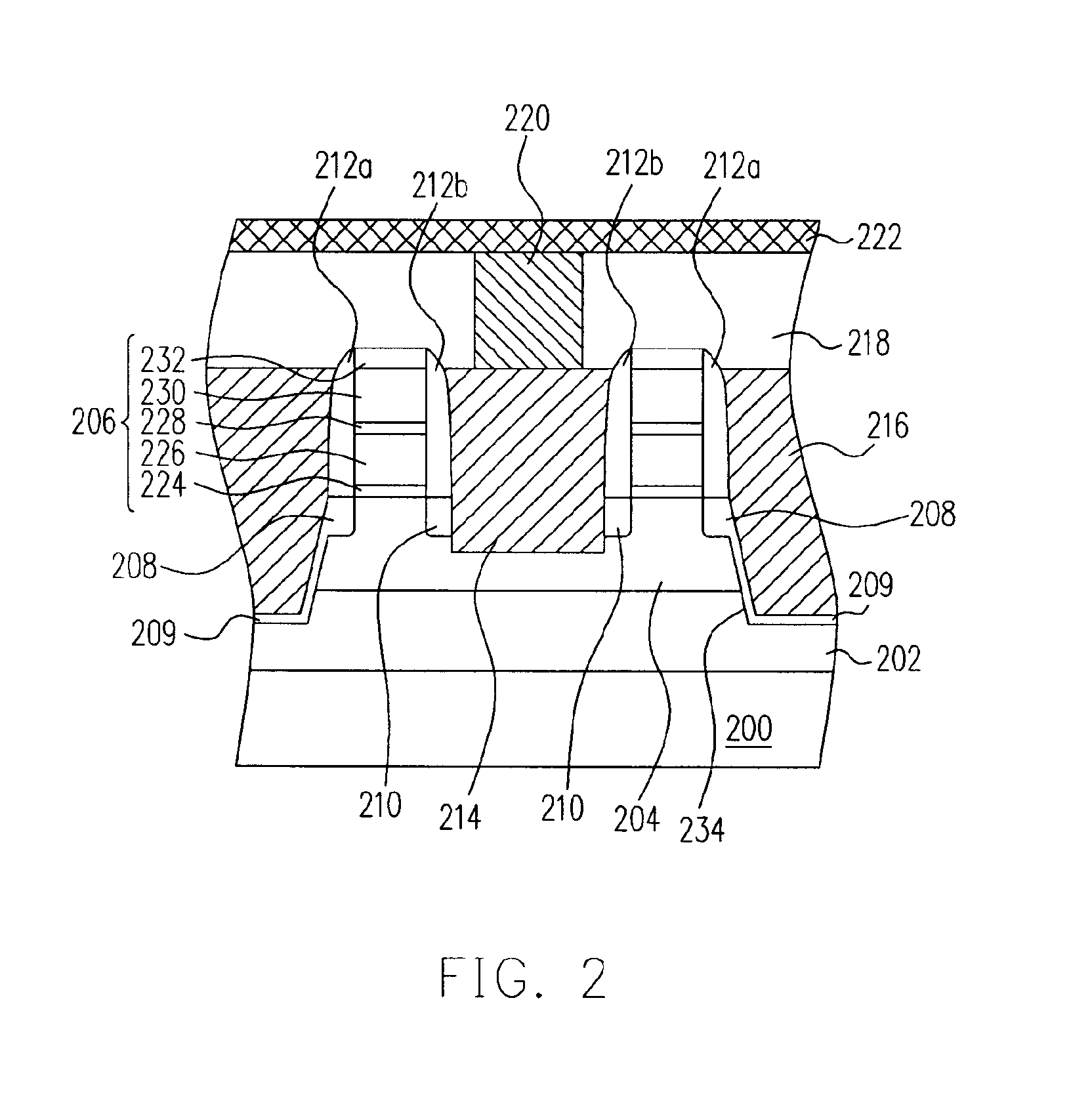
FIG. 2 is a cross-sectional view of a structure of a flash memory device according to an embodiment of the present invention. A BiNOR type of array flash memory device is used as an example to illustrate the features of the present invention.

Referring to FIG. 2, the flash memory device of the present invention is formed with a P-type substrate 200, a deep N-type well region 202, a P-type well region 204, a stacked gate structure 206, a source region 208, a doped region 209, a drain region 210, a spacer 212a, a spacer 212b, a contact window 214, a contact window 216, an interlayer dielectric layer 218, a plug 220 and a conductive line 222. The stacked gated structure 206 is formed with a tunnel oxide layer 224, a floating gate 226, a gate dielectric layer 228, a control gate 230 and a gate cap layer 232.

The P-type substrate 200 comprises a trench 234. The deep N-type well region 202 is located in the P-type substrate. The spacer 212a and the spacer 212b are disposed on the sidewall o...


PUM


Abstract

A flash memory device includes a substrate having a trench, a deep N-type well region in the substrate, a stacked gate structure on the substrate, a first and a second spacer on a sidewall of the stacked gate, wherein the first spacer is connected with the top of the trench, a source region in the substrate under the first spacer, a drain region in the substrate under the second spacer, a P-type well region between the stacked gate and the deep N-type well region, wherein the junction between the two well regions is higher than the bottom of the trench, a doped region along the bottom and the sidewall of the trench, wherein this doped region is connected with the source region and isolates the P-type well region from the contact formed in the trench, the contact being electrically connected to the source region.

Description

BACKGROUND OF INVENTION1. Field of the InventionThe present invention relates to a structure of a non-volatile memory device and a method for fabricating the same. More particularly, the present invention relates to a structure of a flash memory device method and a method for fabricating thereof.2. Description of Related ArtA flash memory device provides the property of multiple entries, retrievals and erasures of data. Moreover, the stored information is retained even electrical power is interrupted. As a result, the non-volatile memory device is widely used in personal computers and electronic systems.A typical flash memory device employs doped polysilicon for the formation of the floating gate and the control gate. During the programming and the erasing of this type of flash memory device, an appropriate voltage is applied to the source region, the drain region and the control gate to inject electrons into and to eject electrons from the polysilicon floating gate.In general, elec...

Claims


Application Information

Patent Timeline
IPC IPC(8): H01L21/70H01L27/115H01L21/8247
CPCH01L27/11521H01L27/115H10B69/00H10B41/30
Inventor HUNG, CHIH-WEISUNG, DACHEN, CHIH-MING
Owner POWERCHIP SEMICON MFG CORP
Why Eureka
Try Eureka