Analog-to-digital conversion and implementations thereof

Active Publication Date: 2010-10-21
SAMSUNG ELECTRONICS CO LTD
View PDF6 Cites 16 Cited by
  • Summary
  • Abstract
  • Description
  • Claims
  • Application Information

AI Technical Summary

Benefits of technology

[0016]A further embodiment includes an ADC configured to perform a conversion process that includes at least a first step and a second step. The first step is performed based on a first ramp signal having a first slope, and the second step is performed

Problems solved by technology

The problem with the ramp ADC is that it must step through, one value at a time, all possible digital values that could be generated and output by the ADC.
Unfortunately, the ramp signals during the course and fine A

Method used


Image

  • Analog-to-digital conversion and implementations thereof
  • Analog-to-digital conversion and implementations thereof
  • Analog-to-digital conversion and implementations thereof

Examples


Example

First Embodiment

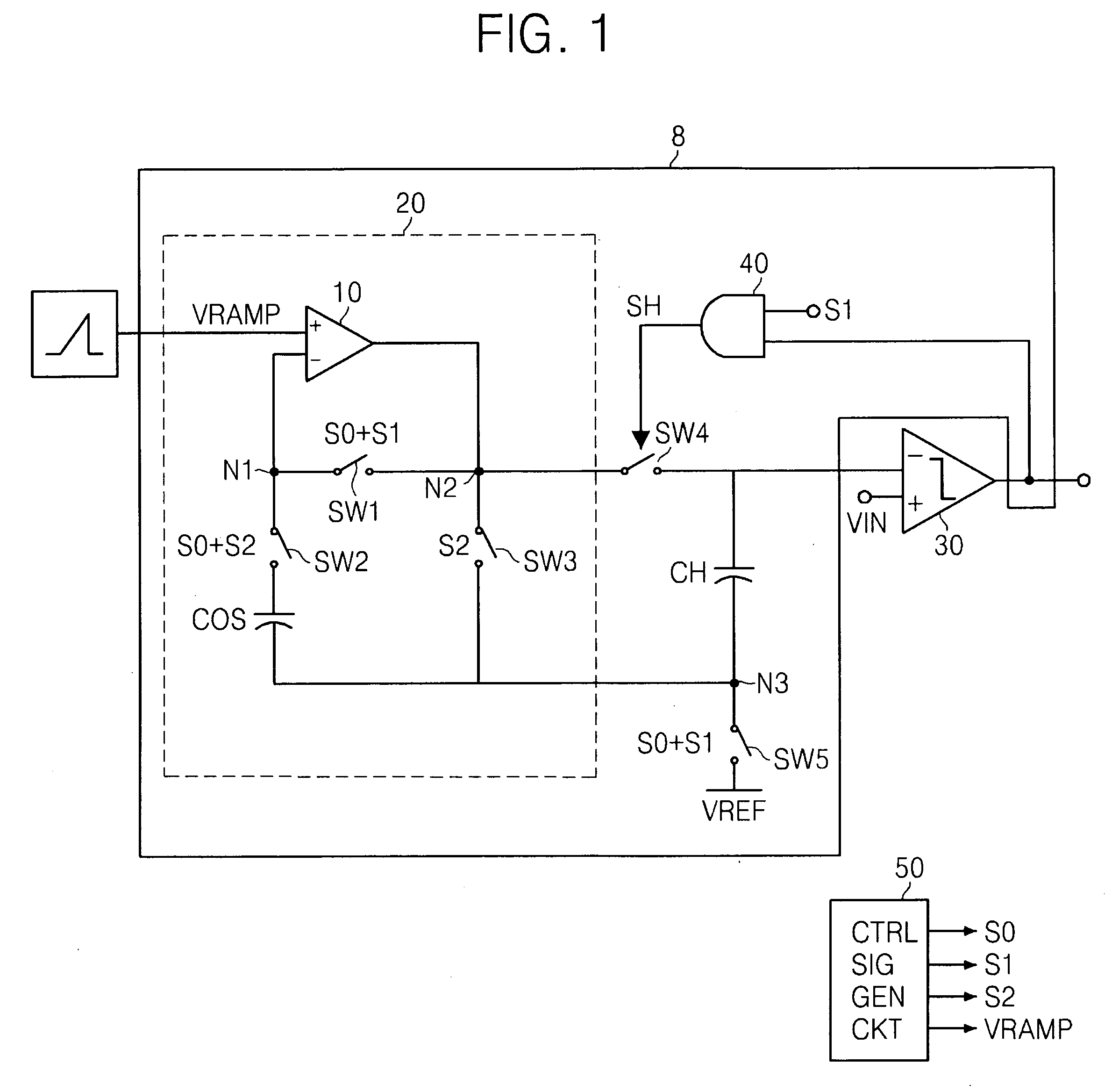
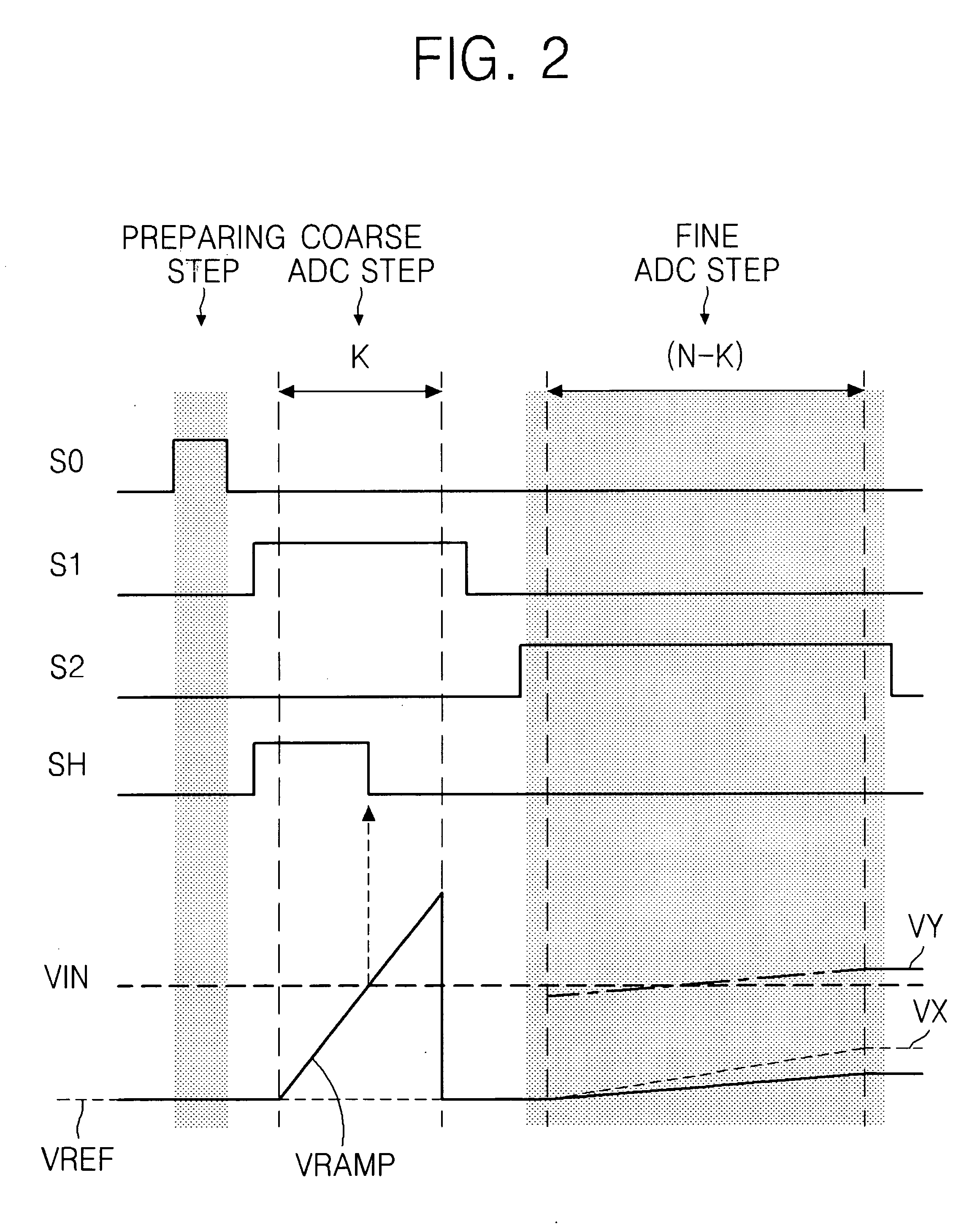
[0039]FIG. 1 illustrates an analog-to-digital converter (ADC) according to an embodiment of the present invention. As shown, the ADC includes a supply circuit 8. The supply circuit 8 supplies a reference voltage VY to a negative input terminal of an operational amplifier 30. The operational amplifier 30 compares this reference voltage VY to the voltage VIN of an input signal supplied to the positive input terminal.

[0040]The supply circuit includes a first differential amplifier 10, first-fifth switches SW1-SW5, first and second capacitors COS and CH, and NAND gate 40. The first differential amplifier 10 receives a ramp voltage VRAMP at a positive terminal, and the negative terminal is connected to a first node N1. The output of the first differential amplifier 10 is supplied to a second node N2. The first node N1 and the second node N2 are selectively connected by a first switch SW1. The first switch SW1 opens or closes based on a first control signal S0 and a second...

Example

Second Embodiment

[0062]FIG. 6 illustrates an analog-to-digital converter (ADC) according to another embodiment of the present invention. As shown, the ADC includes a supply circuit 8′. The supply circuit 8′ supplies a reference voltage VY to a negative input terminal of an operational amplifier 30. The operational amplifier 30 compares this reference voltage VY to the voltage VIN of an input signal supplied to the positive input terminal.

[0063]The supply circuit 8′ includes a first differential amplifier 10, first, fourth, and sixth-tenth switches SW1, SW4, SW6-SW10 and first and second capacitors COS and CH, and NAND gate 40. The first differential amplifier 10 receives the ramp voltage VRAMP at the positive terminal, and the negative terminal is connected to the first node N1. The output of the first differential amplifier 10 is supplied to the second node N2. The first node N1 and the second node N2 are selectively connected by the first switch SW1. The first switch SW1 opens or ...

Example

Third Embodiment

[0075]FIG. 10 illustrates an ADC according to a further embodiment of the present invention. As shown, in the ADC in this embodiment, the supply circuit 80 is controlled by first, second, third, fourth and fifth control signals S0-S4. In the supply circuit 80, a first switch 100 is connected between a first node D1 and the negative terminal of an operational amplifier 108. The first switch 100 receives the ramp signal VRAMP at the first node D1, and is controlled by a fifth control signal S4. In particular, when the fifth control signal S4 is logic high, the first switch 100 is closed; and when the fifth control signals S4 is logic low, the first switch 100 is open. A second switch 102 is connected between the first node D1 and a second node D2, and receives the ramp signal VRAMP at the first node D1. The second switch 102 is controlled by the first, third and fourth control signals. In particular, if any of the first, third and fourth control signals S0, S2 and S3 a...


PUM


Abstract

In one embodiment, an analog-to-digital converter (ADC) includes a comparator and a supply circuit. The comparator is configured to compare an input signal to a reference signal. The supply circuit is configured to supply the reference signal. The supply circuit is configured to provide different circuit configurations for supplying the reference signal during different stages of analog-to-digital conversion such that the reference signal is scaled in substantially a same manner during at least two of the stages.

Description

PRIORITY STATEMENT[0001]This application claims the benefit of priority under 35 U.S.C. §119 to Korean Patent Application No. 10-2009-0034257, filed on Apr. 20, 2009, in the Korean Intellectual Property Office, the entire contents of which is incorporated herein by referenceBACKGROUND[0002]1. Field[0003]The present invention relates to analog-to-digital conversion.[0004]2. Description of the Related Art[0005]Many devices produce an analog signal that must then be converted to a digital signal for digital processing. For example, many sensors generate an analog signal that must be converted to digital before being handled by a computer.[0006]As another example, a CMOS image circuit includes an array of pixels that output analog signals. These analog signals are then converted to digital. Many CMOS image sensors use a ramp analog-to-digital converter (ADC), which is essentially a comparator and appropriate control logic. In the conventional ramp ADC, an input voltage of the signal to ...

Claims


Application Information

Patent Timeline
IPC IPC(8): H03M1/12
CPCH03M1/1225H03M1/56H03M1/144H03M1/12H04N25/00
Inventor LEE, JEONGHWANHAN, GUNHEEYOO, KWI SUNGHAM, SEOG HEON
Owner SAMSUNG ELECTRONICS CO LTD
Why Eureka
Try Eureka