Micropackaging method and devices

a technology of micro-packaging and components, applied in the direction of micro-structural devices, micro-structural technology, micro-structural device assembly, etc., can solve the problems of incompatibility between the ceramic in the packaging casing and the components inside, the process has inherent drawbacks, and the inability to make very thin walls of such ceramic materials, so as to simplify the manufacturing process and reduce costs

Inactive Publication Date: 2010-03-04
SILEX MICROSYST
View PDF29 Cites 26 Cited by
  • Summary
  • Abstract
  • Description
  • Claims
  • Application Information

AI Technical Summary

Benefits of technology

[0011]The present invention provides a method of micro-packaging a component. At least a first and second substrate is provided of which the first substrate is a semiconductor substrate being provided with at least one electrical through connection. A compartment is formed in either one or a plurality of the substrates by etching. A component is provided above the first semiconductor substrate so that it covers the at least one through wafer connections and will be located within the compartment. The component is connected to at least one through wafer connection and the substrates are joined to form a sealed micro-packaged device. P There may also be provided a plurality of through wafer connections. Preferably the substrates are semiconductor substrates. Preferably the substrates comprising through wafer connections are thick enough to easily be handled during the manufacturing.
[0014]Hermetic sealing can be made at wafer-level using wafer bonding which significantly simplifies the manufacturing process thereby reducing costs.
[0015]Furthermore, a higher density of vias is possible in silicon based packages by using photolithography and etching processes than possible by using mechanical machining processes.

Problems solved by technology

These processes have inherent drawbacks.
Also, it is difficult to make very thin walls in such ceramic materials.
Furthermore, there will be material incompatibility between the ceramic in the casing of the package and the components inside, which often are silicon based, as for example MEMS (Microelectromechanical Systems) devices.
Differences in e.g. thermal expansion coefficients can cause artefacts.

Method used


Image

  • Micropackaging method and devices
  • Micropackaging method and devices
  • Micropackaging method and devices

Examples


Embodiment Construction

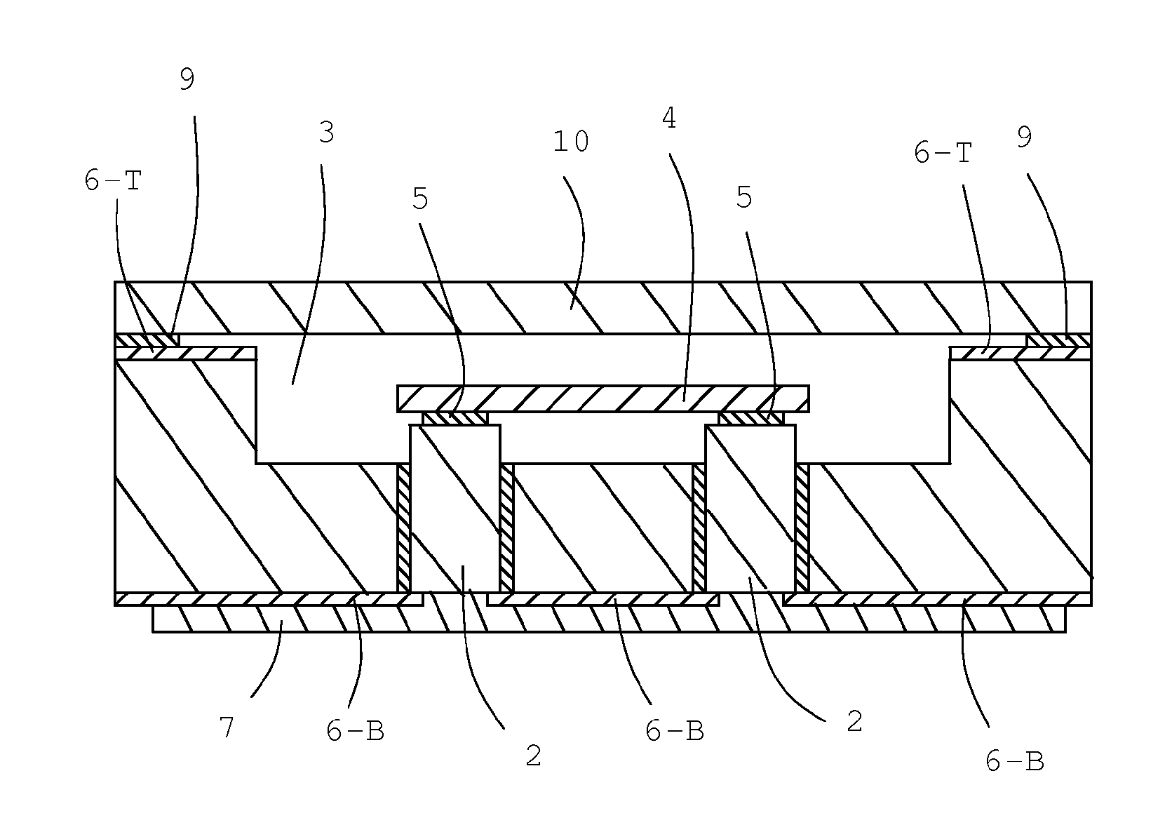
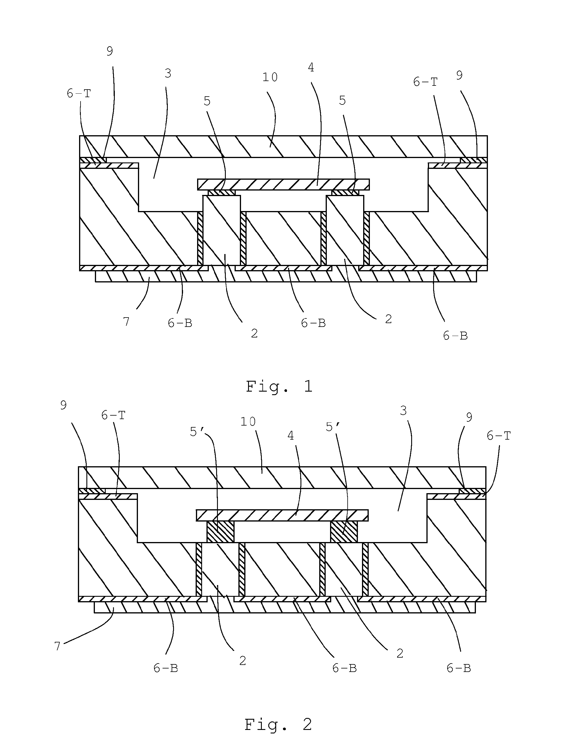
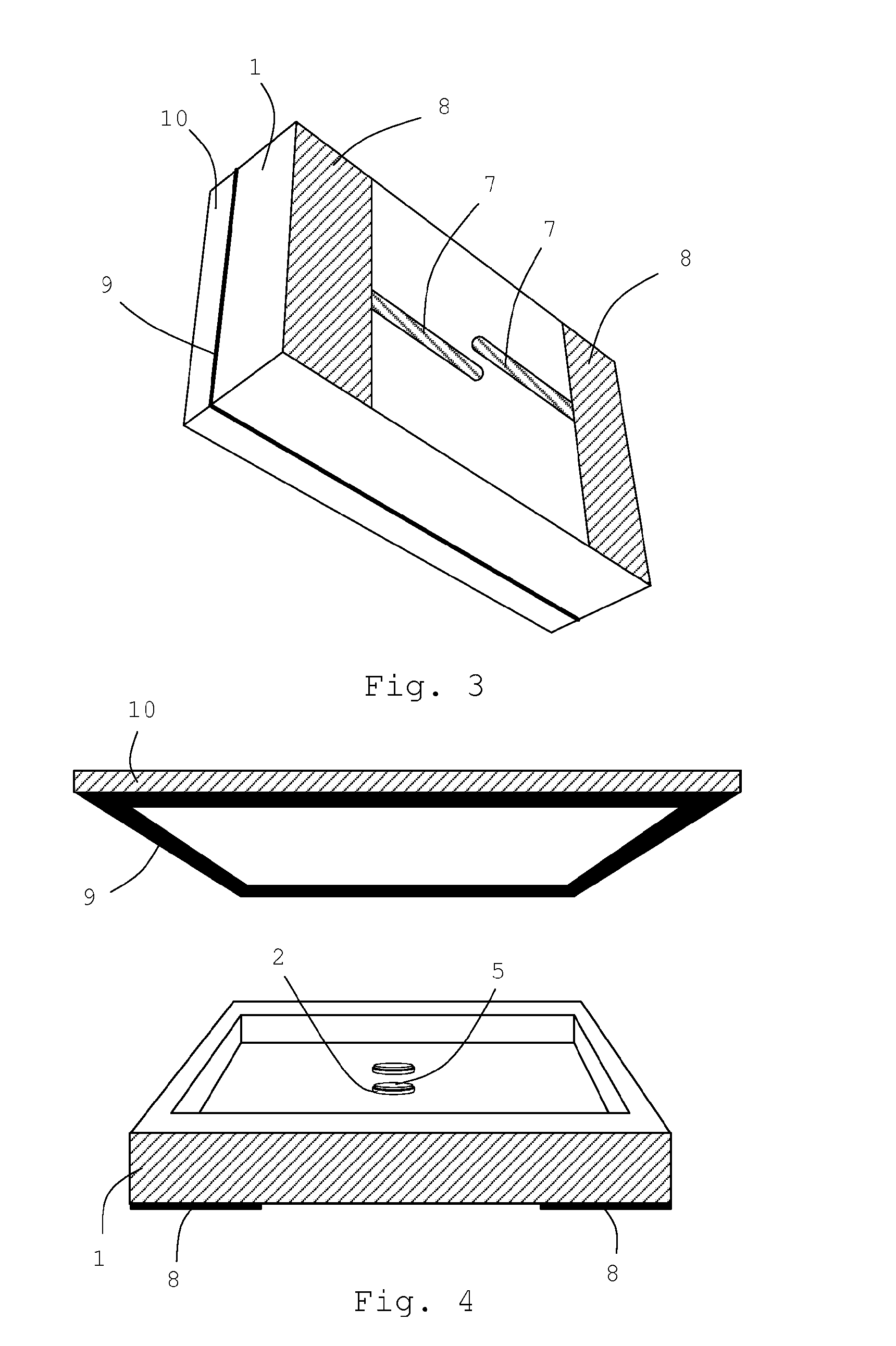
[0037]The invention is based on the use of electrical through connections (or “vias”), which enables connection of packaged micro-components to circuit boards or to other components with the provision of bulky connector legs or pins, and wafer-level hermetic encapsulation. The terms electrical through connection and via are interchangeably used in this application.

[0038]Preferably the starting wafers having said vias are semiconductor wafers, more preferably single crystalline silicon wafers, however not limited to this. The term “semiconductor wafer” also comprises other wafer materials typically used in the field, such as glass wafers and ceramic wafers. The terms wafer and substrate are interchangeably used throughout this application since processing preferably is made on wafer level, i.e. many devices are manufactured in parallel.

[0039]Preferably, the packaged component is made by using a wafer having been provided with vias in accordance with the teachings of the International...


PUM


Abstract

A method of micro-packaging a component wherein at least a first and a second semi-conductor substrate are provided, one of which has electrical through connections (vias). A depression in either one of the substrates or in both is etched. A component is provided above vias and connected thereto. The substrates are joined to form a sealed package. A micro-packaged electronic or micromechanic device, including a thin-walled casing of a semi-conductor material having electrical through connections through the bottom of the casing is also disclosed. An electronic or micromechanic component is attached to the electrical through connections, and the package is hermetically sealed for maintaining a desired atmosphere, suitably vacuum inside the box.

Description

TECHNICAL FIELD [0001]The present invention relates to packaging of components for electronic devices, in particular devices requiring small components, such as but not limited to electrical and micromechanical surface micromachined oscillators for computers, mobile phones and the like.BACKGROUND OF THE INVENTION [0002]Certain components for surface mounting on circuit boards must be packaged in protective casings, quite often in vacuum or other controlled atmosphere / ambient and also need to be provided with connector legs for mounting or solder bumps for surface mounting. Today most encapsulating casings are made of polymers or ceramic materials. The latter is commonly used for packaged components that are hermetically sealed.[0003]The inner compartment of such ceramic casings is made by milling processes. These processes have inherent drawbacks.[0004]One thing is that the thickness of the package has an inherent lower limit. For e.g. mobile phone applications thickness is a vital ...

Claims


Application Information

Patent Timeline
Patent Type & Authority Applications(United States)
IPC IPC(8): H01R9/00H01L21/302H10K39/10H10K59/90
CPCH01L21/762H01L21/823481H01L2924/1461H01L23/147H01L23/055H01L23/49838H01L23/552H01L23/66H01L2223/6622H01L2223/6688H01L2924/09701H01L2924/1433H01L2924/3011H01L2224/16225H01L2924/01322B81C1/00246H01L2924/00H01L2924/00014H01L23/26H01L2224/16235H01L2924/15153H01L2924/16195H01L2924/16251H01L2924/00011H01L2224/0401B81B7/0077B81C3/008H01L23/04H01L23/06H01L25/10
Inventor EBEFORS, THORBJORNKALVESTEN, EDVARDBAUER, TOMAS
Owner SILEX MICROSYST
Why Eureka
Try Eureka