Wafer processing method

Active Publication Date: 2010-03-04
DISCO CORP
View PDF0 Cites 24 Cited by
  • Summary
  • Abstract
  • Description
  • Claims
  • Application Information

AI Technical Summary

Benefits of technology

[0007]It is therefore an object of the present invention to provide a wafer processing method which can reliably remove the peripheral marginal area where the annular reinfor

Problems solved by technology

However, such a reduction in wafer thickness to 50 μm or less causes easy damage to the wafer, so that handling such as transportation of the wafer is difficult.
In dividi

Method used


Image

  • Wafer processing method
  • Wafer processing method
  • Wafer processing method

Examples


Embodiment Construction

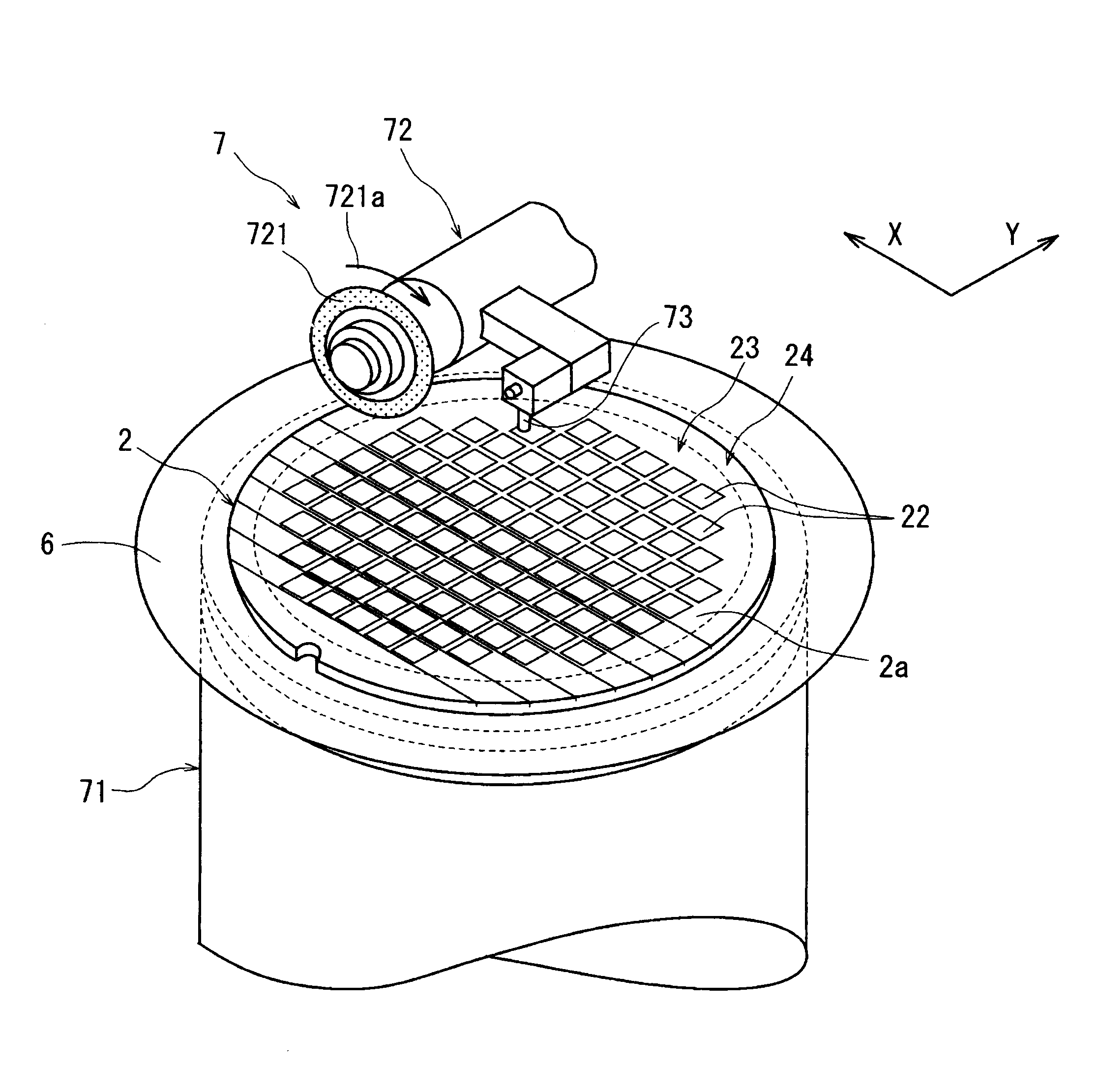
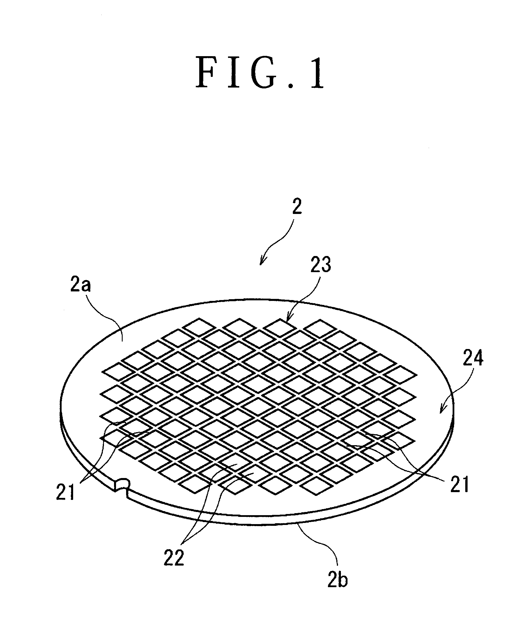
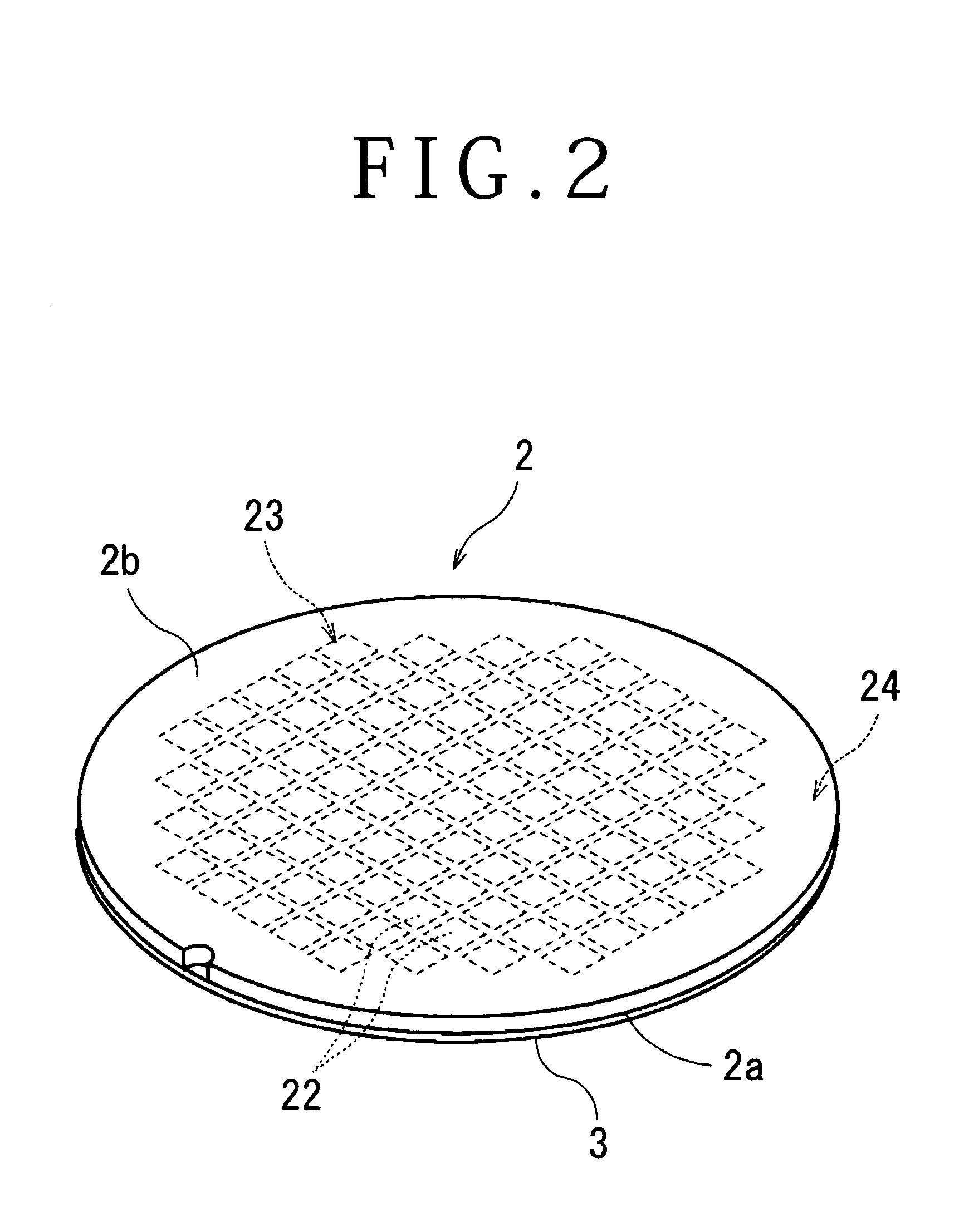
[0032]Some preferred embodiments of the wafer processing method according to the present invention will now be described in detail with reference to the attached drawings. FIG. 1 is a perspective view of a semiconductor wafer 2 as a wafer to be divided into individual devices by the wafer processing method according to the present invention. The semiconductor wafer 2 shown in FIG. 1 is a silicon wafer having a thickness of 700 μm, for example. The semiconductor wafer 2 has a front side 2a and a back side 2b. A plurality of crossing streets 21 are formed on the front side 2a of the semiconductor wafer 2 to thereby partition a plurality of rectangular regions where a plurality of devices 22 such as ICs and LSIs are respectively formed. The semiconductor wafer 2 includes a device area 23 where the devices 22 are formed and a peripheral marginal area 24 surrounding the device area 23.

[0033]Prior to cutting the semiconductor wafer 2 along the streets 21 to divide it into the individual d...


PUM


Abstract

Disclosed herein is a wafer processing method for dividing a wafer along a plurality of streets. The wafer processing method includes a back grinding step of grinding the back side of the wafer in an area corresponding to a device area to thereby reduce the thickness of the device area to a predetermined finished thickness and to simultaneously form an annular reinforcing portion on the back side of the wafer in an area corresponding to a peripheral marginal area, a wafer supporting step of attaching the back side of the wafer to a dicing tape, a kerf forming step of cutting the front side of the wafer along each street to thereby form a kerf having a depth corresponding to the thickness of the device area along each street, thereby dividing the device area into individual devices, and a peripheral marginal area removing step of peeling off the peripheral marginal area from the dicing tape.

Description

BACKGROUND OF THE INVENTION[0001]1. Field of the Invention[0002]The present invention relates to a wafer processing method for dividing a wafer along a plurality of crossing streets formed on the front side of the wafer, the wafer having a device area and a peripheral marginal area surrounding the device area, the device area being composed of a plurality of regions partitioned by the streets, wherein individual devices are respectively formed in the regions of the device area.[0003]2. Description of the Related Art[0004]In a semiconductor device fabrication process, a plurality of crossing division lines called streets are formed on the front side of a substantially disk-shaped semiconductor wafer to thereby partition a plurality of regions where devices such as ICs and LSIs are respectively formed. The semiconductor wafer is cut along these streets to thereby divide a device area into the individual devices. Prior to cutting the wafer along the streets, the back side of the wafer ...

Claims


Application Information

Patent Timeline
IPC IPC(8): H01L21/78
CPCH01L21/6835H01L21/6836H01L2221/68336H01L2221/68327H01L21/78
Inventor KAJIYAMA, KEIICHIKONDO, AZUMI
Owner DISCO CORP
Why Eureka
Try Eureka