Method for fabricating an integrated circuit

a technology of integrated circuits and manufacturing methods, applied in the direction of basic electric elements, semiconductor/solid-state device manufacturing, electric apparatus, etc., can solve the problems of rc delay becoming the dominant factor, not normally used in semiconductor manufacturing,

Inactive Publication Date: 2010-03-04
NAN YA TECH
View PDF9 Cites 262 Cited by
  • Summary
  • Abstract
  • Description
  • Claims
  • Application Information

AI Technical Summary

Benefits of technology

[0008]It is one objective of the present invention to provide an improved method for forming a

Problems solved by technology

However, under the increased IC speed and the device density, the RC delay becomes the dominant factor.
While the aforesaid materials respectively have a relatively low dielectric constant, they are n

Method used


Image

  • Method for fabricating an integrated circuit
  • Method for fabricating an integrated circuit
  • Method for fabricating an integrated circuit

Examples


Embodiment Construction

[0012]Without the intention of a limitation, the invention will now be described and illustrated with reference to the preferred embodiments of the present invention.

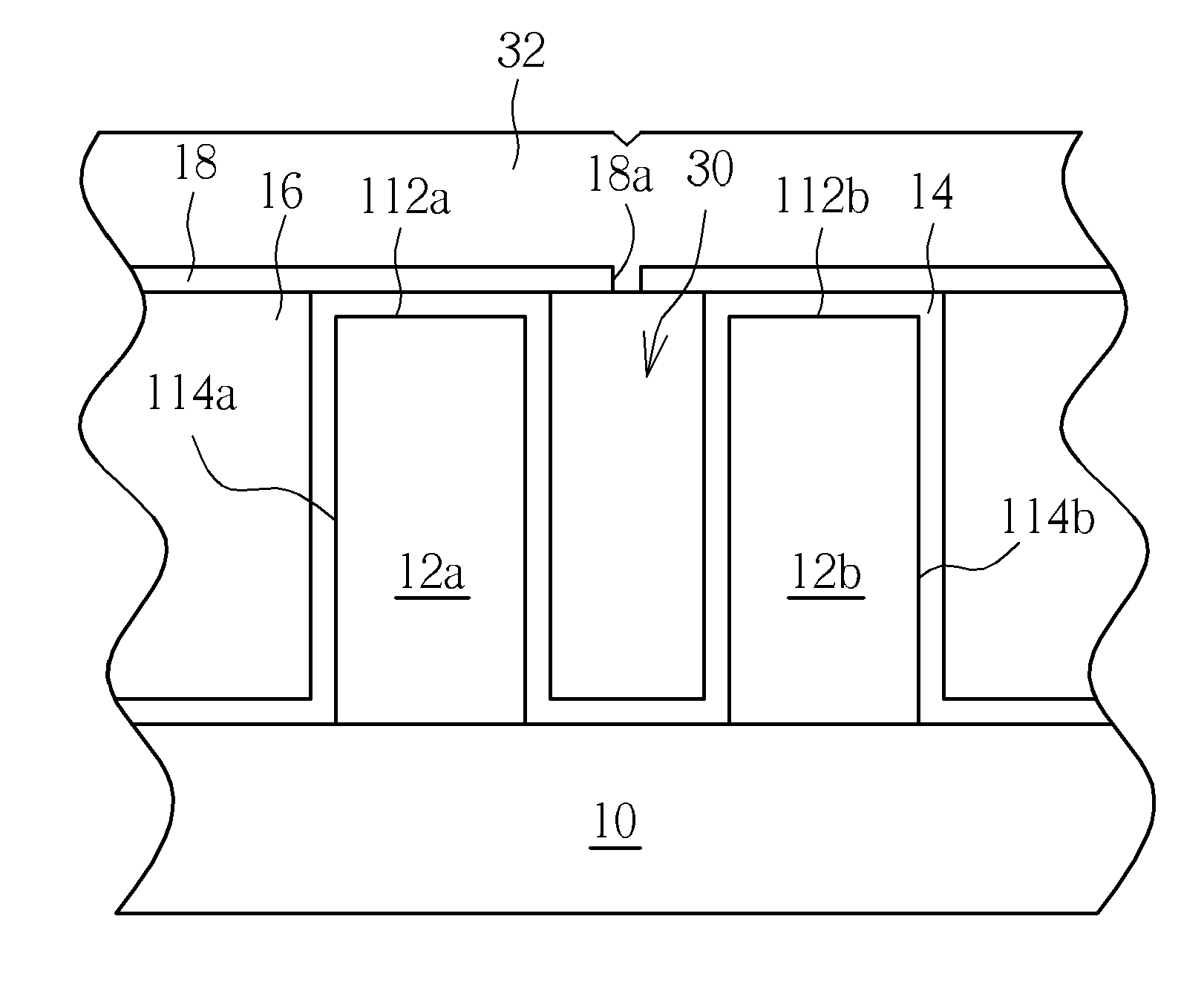
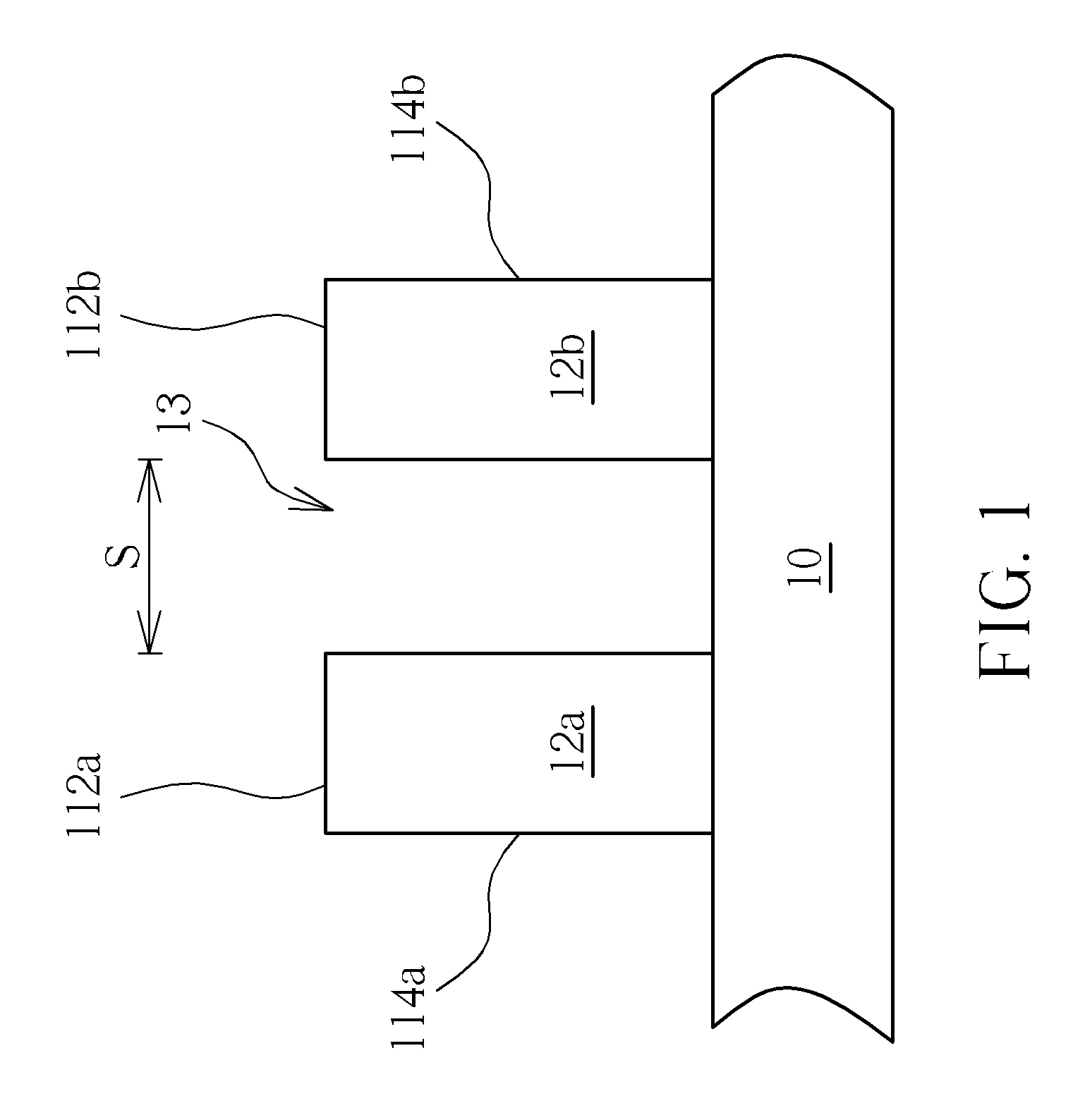
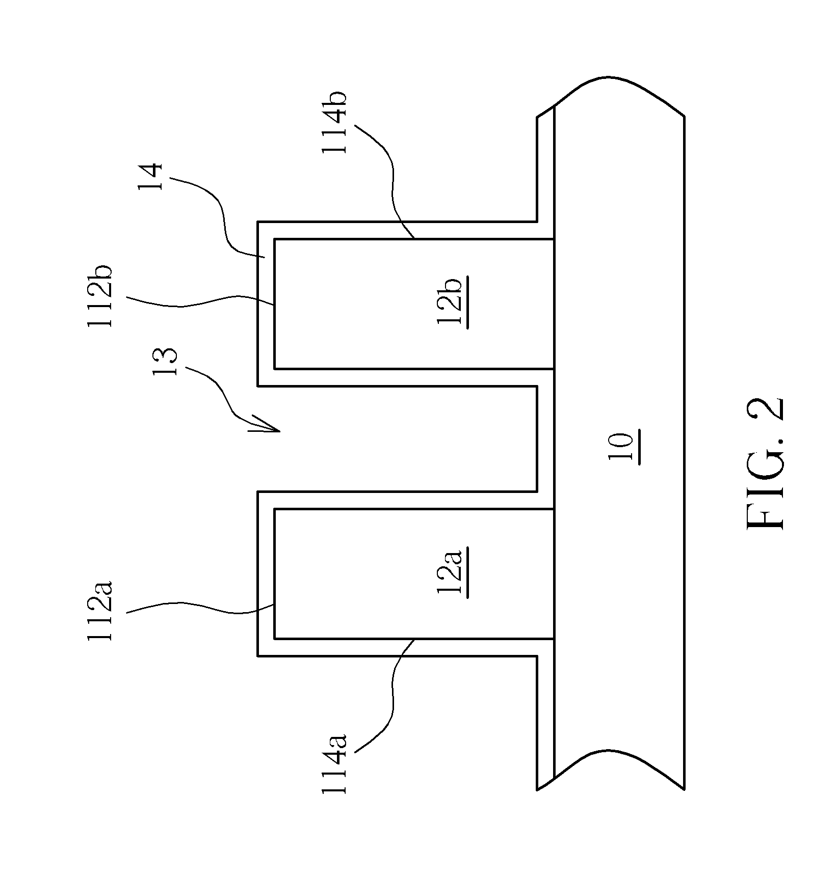
[0013]FIG. 1 to FIG. 8 are schematic, cross-sectional diagrams showing a method for fabricating an integrated circuit in accordance with the preferred embodiment of this invention. As shown in FIG. 1, a substrate 10 is provided. A first conductive wire 12a and a second conductive wire 12b are provided on the substrate 10. The first conductive wire 12a is adjacent to the second conductive wire 12b. For example, a space (S) between the first conductive wire 12a and the second conductive wire 12b ranges between 30 nanometers and 500 nanometers. According to this embodiment of the present invention, the first and second conductive wires 12a and 12b are both composed of metal such as aluminum, but not limited thereto.

[0014]It is understood that in other embodiments the first and second conductive wires 12a and 12b may be com...


PUM


Abstract

A method for fabricating an integrated circuit is provided. A substrate having thereon a first conductive wire and a second conductive wire is provided. A liner is formed on the first conductive wire and second conductive wire. An ashable material layer is filled into a gap between the first conductive wire and second conductive wire. The ashable material layer is then polished to expose a portion of the liner. A cap layer is formed on the ashable material layer and on the exposed liner. A through hole is etched into the cap layer to expose a portion of the ashable material layer. Thereafter, the ashable material layer is removed by way of the through hole.

Description

BACKGROUND OF THE INVENTION[0001]1. Field of the Invention[0002]The present invention relates, in general, to a method for fabricating an integrated circuit. More particularly, the present invention relates to a method for fabricating an integrated circuit with an air gap.[0003]2. Description of the Prior Art[0004]Semiconductor manufacturers have been trying to shrink transistor size in integrated circuits (IC) to improve chip performance, which leads to the result that the integrated circuit speed is increased and the device density is also greatly increased. However, under the increased IC speed and the device density, the RC delay becomes the dominant factor.[0005]To facilitate further improvements, semiconductor IC manufacturers have been driven by the trend to resort to new materials utilized to reduce the RC delay by either lowering the interconnect wire resistance, or by reducing the capacitance of the inter-layer dielectric (ILD). A significant improvement is achieved by rep...

Claims


Application Information

Patent Timeline
IPC IPC(8): H01L21/44
CPCH01L21/76834H01L21/7682
Inventor CHANG, SHUO-CHEKUO, CHI-HSIANG
Owner NAN YA TECH
Why Eureka
Try Eureka